
Designing and testing a low-noise amplifier – Part 1
There are plenty of amplifier designs available online. You can simply purchase one and be done with whatever you plan on doing. However, designing your own low-noise amplifier can be fun. For someone into HAM radio, you might have come across weather satellite LRPT reception using an RTL-SDR. Receiving images from a satellite may require a good low-noise amplifier. On the other hand, someone into radio astronomy definitely requires a very low noise amplifier to receive the hydrogen line frequency emanating from the milky way.
In this blog post, I show how I designed a low-noise amplifier having bias-tee for power delivery through coaxial cable and an arrangement for bandpass filter.
The specifications
Before everything else, let’s go through the specifications. The noise figure of an LNA should be as low as possible. For this design, I require the noise figure of less than 1dB. Being an amplifier, it needs to have some power gain to drive through long cables because I would be installing it far away from my receiver. Therefore, a gain of 15-20dB should be fine by me. Finally, the LNA should be as linear as possible with OIP3 >30dBm.
Now that we have some specifications in hand. I start looking for suitable amplifier chips. As a result, I came across several amplifiers. Some were expensive, some quite affordable. Having used PSA-5043+ before, I had good experience using it and also learnt an important lesson while using this amplifier. PSA-5043+ is an excellent amplifier with OIP3 of ~30dBm. On the other hand, another amplifier I found called PGA-103+ comes with OIP3 of ~40dBm. A 10dB improvement in linearity makes our choice very clear. I am preferring the PGA-103+ over PSA-5043+.
Other companies make LNA too, but none of them are as affordable and wideband as Minicircuits.
The PGA-103+ comes with a gain of 22dB at 400MHz and rolls off down to 8dB at 3GHz. Now, this amplifier is quite good all the way to 2GHz if you care about the gain. Whereas the noise figure remains down to 1dB at 3GHz. I plan on using this LNA for LRPT reception which happens in the VHF band (137MHz). Therefore, I am more than okay with this performance.
Additionally, I also need an option for band pass filter for preselection. This band pass filter should cover the LRPT frequencies and 2m ham band.
The design
Based around the PGA-103+, I prepared a schematic for the LNA circuit. The entire circuit is divided into 3 major parts.
- The bias tee to power the board through coaxial cable
- Band pass filter
- The LNA (PGA-103+)
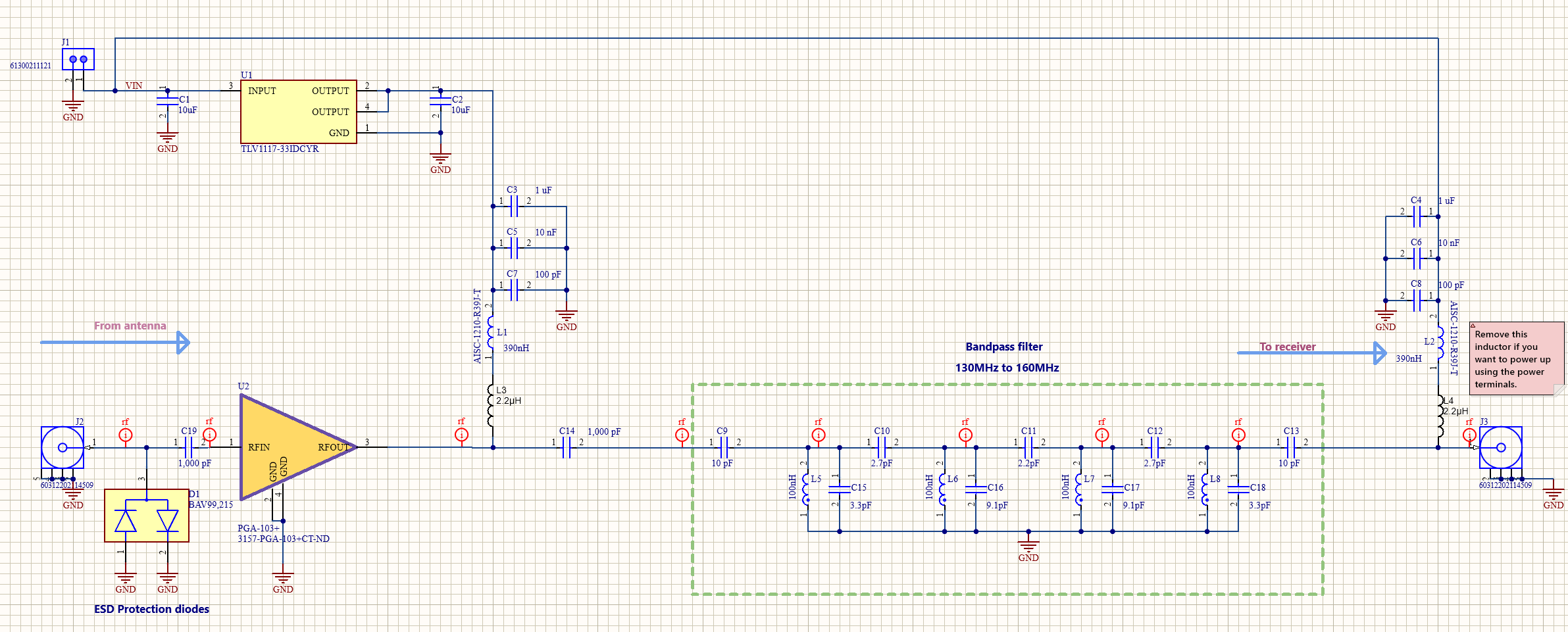
Let’s look at each section in detail.
Bias-tee
The bias-tee after the band pass filter powers the entire board. We would need to inject DC on the coaxial line through another bias-tee near the receiver. This DC would then be extracted by the bias tee on the LNA circuit and used to power up the amplifier. The following block diagram explains the system much better than words do.
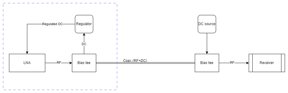
Looking at the schematic, components L4, L2, C8, C6, and C4 form the bias tee responsible for extracting DC from the coaxial line. The extracted DC then feeds the linear regulator TLV1117-3.3 which further generates 3.3V DC to power the PGA-103+ amplifier. Finally, the regulated 3.3V DC passes through another bias tee that biases the amplifier.
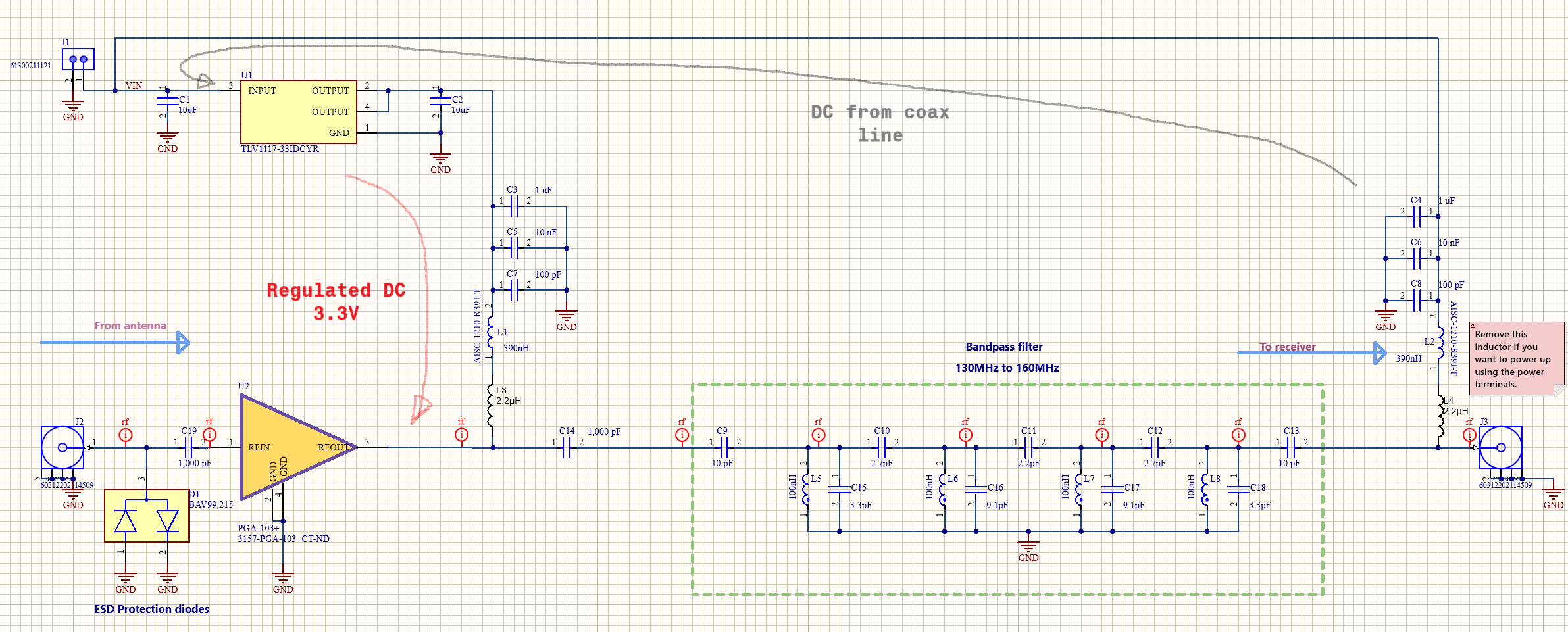
In short, the bias tee near the connector J3 (output SMA connector) extracts the DC from the coax line, feeds the regulator and biases the LNA through the second bias tee.
Bias tee design
A bias tee must ideally block all RF from entering the DC path. Inductor is the only known component that does the job of allowing DC and blocking RF. This phenomenon is explained through the concept of inductive reactance.
\(X_L = 2 \pi fL\)
The inductor touching the RF line should exhibit an inductive reactance high enough to prevent RF from leaking into the DC path. It may so happen that the inductor chosen may have high inductive reactance at higher frequencies but not so much for the lower frequencies. To prevent this, why not select a large inductor?
For example, an inductor of 10uH should exhibit a reactance of \(628 k \Omega \) at 100MHz. While, the same inductor exhibits a reactance of \(62.8 k \Omega\) at 10MHz.
Although a larger inductor might work well for lower frequencies, it doesn’t always perform well at higher frequencies due to a phenomenon called the self-resonant frequency (SRF). SRF occurs when the parasitic capacitance between the inductor’s windings causes it to resonate. The resonance frequency is given by:
\( f_r = \frac{1}{2 \pi \sqrt{LC}} \).
Above the SRF, the inductor can no longer block RF effectively, allowing it to leak into the DC path. The SRF decreases as the inductance increases, meaning lower-value inductors tend to have higher SRFs. Therefore, using smaller inductors in series can help extend the bandwidth of the bias tee. For instance, I’ve selected two inductors in series: one with a value of 2.2 µH and an SRF of 200 MHz, and another with a value of 390 nH and an SRF of 510 MHz. This combination should ensure acceptable performance up to at least 500 MHz.
If we look at their datasheets, the 2.2uH part has a SRF of 200MHz. Whereas, the 390nH part has a SRF of 510MHz. Therefore, the bias-tee should provide acceptable performance up to 500MHz minimum.
While I have given an overview of the bias-tee concept, if you wish to explore further, follow this link to microwaves101.
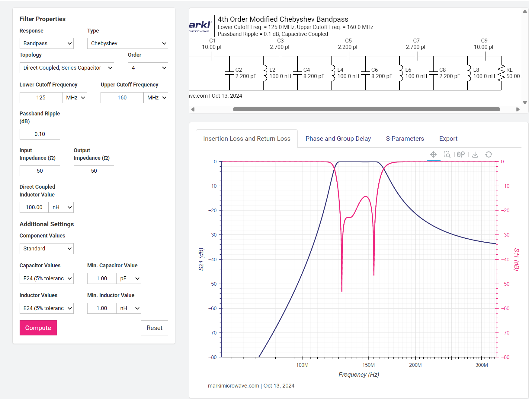
Filter design
Honestly, I did not take much effort into designing the filter. The online filter design tools are quite good and provide usable results. For this project, I used the Marki Microwave’s online LC filter design tool. I entered the cut off frequencies, the order of the filter I need and filter specifications such as ripple level and so on.
It also gives an option to fix the inductor and calculate rest component values. Image below shows the filter design generated by the calculator.
The LNA
Finally, the LNA, PGA-103+ is simple to use. All it needs is 3.3V to 5V biasing which we are providing through the regulator. I mentioned earlier that I used a similar LNA with part number PSA-5043+. There’s one thing I learnt from using that LNA that I would like to implement here; input protection.
My old LNA design did not have input protection and often went bad due to ESD. These parts quite sensitive to ESD and go bad easily. A pair of diodes in anti-parallel configuration should fix this problem effortlessly. I used the BAV-99 which has two diodes in a single package. A lot of popular LNA designs available across the internet use BAV-99 for input protection.
Filter first or LNA first
The usual way is to place the LNA before anything else to maintain lowest achievable noise figure. So, when do we place the filter before the LNA?
In cases of very strong out-of-band interference, a good band pass filter really helps prevent the LNA from saturating and producing unwanted frequency products. For example, if you live close to a commercial FM broadcast transmitter, the strong FM signals will really mess with every signal. It may produce images or simply saturate your amplifier. Only in such cases, a filter before the LNA becomes necessary.
On the other hand, you may require multiple cascaded amplifiers in your front-end for receiving the hydrogen line frequency. However, there still is a chance that the second stage may saturate due to relatively strong FM signal. For such an instance, a filter after the first stage proves to be useful.
Always ensure the LNA is the first thing a signal sees after being picked by an antenna. Why? Because the noise figure of the first stage dominates the system noise figure. Therefore, in my design I have the LNA first and then the filter.
The PCB design
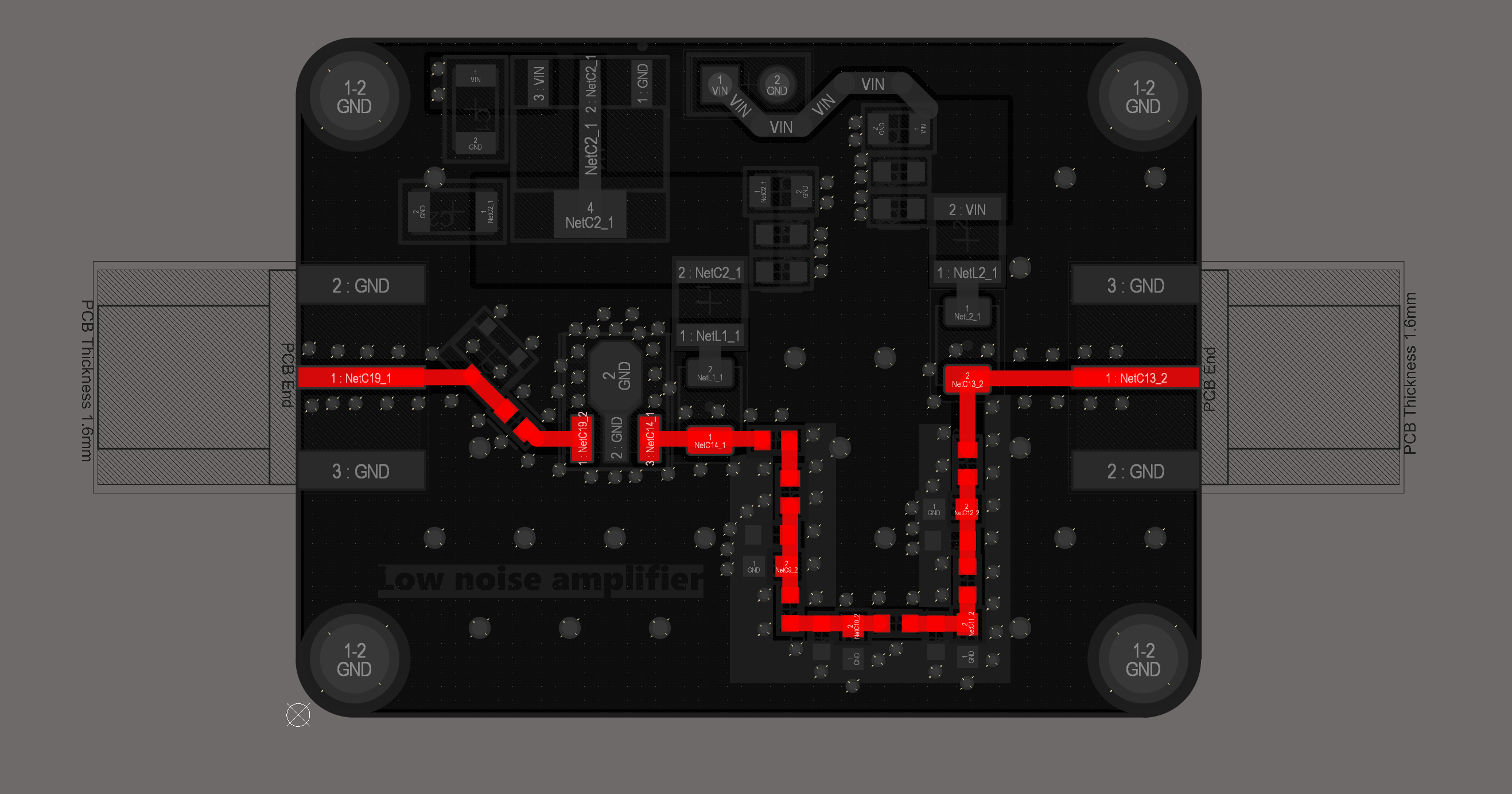
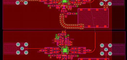
While designing the PCB, the RF nets need special attention with respect to impedance matching. Additionally, the filter layout plays and important role too. A poor filter placement deviates the response from the theoretical design.
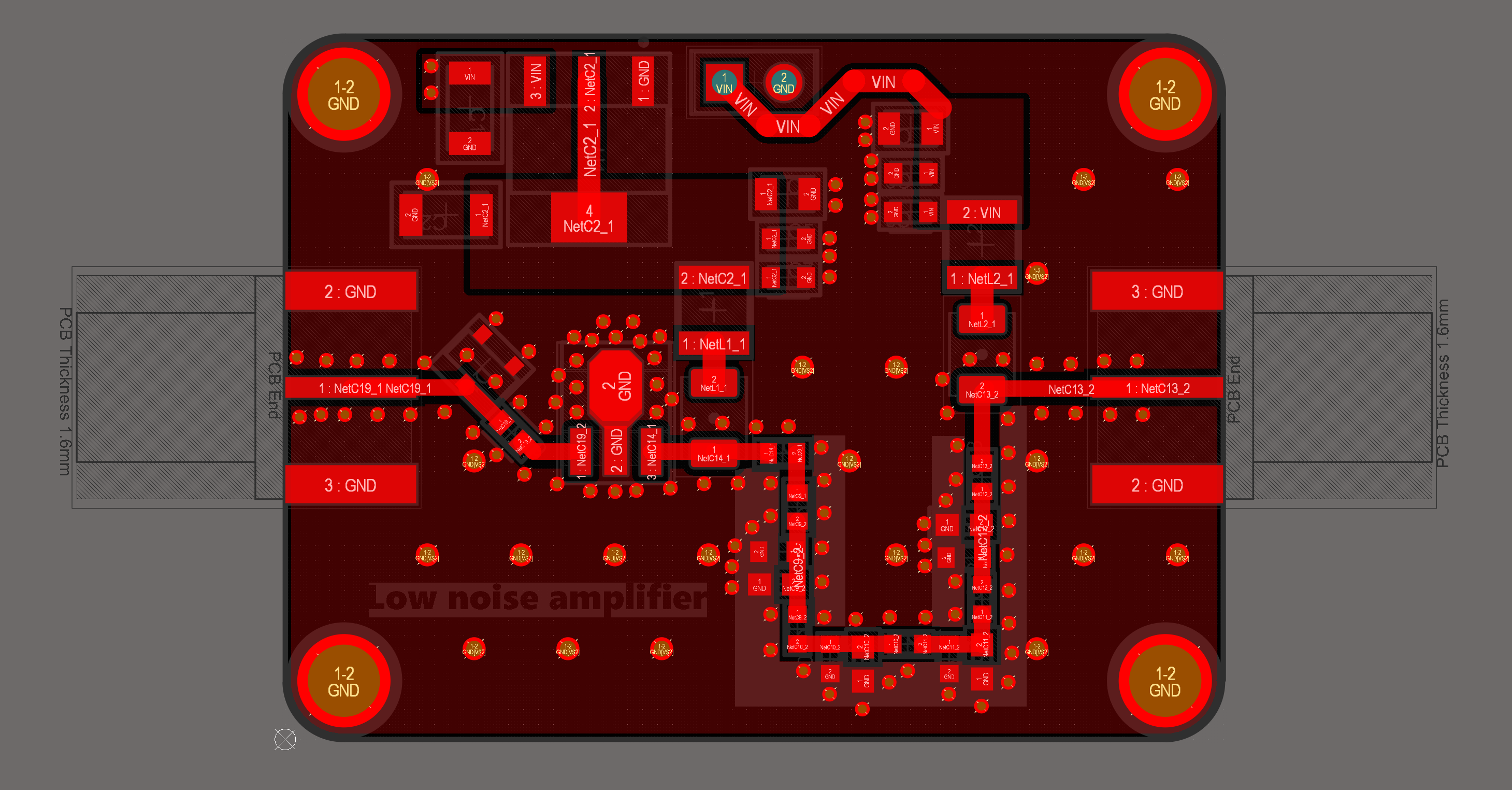
I started the PCB design by defining the mechanical outline of the PCB. The board measures 40mm in width and 30mm in height with two SMA female connectors on both the edges.
I preferred to use coplanar waveguide for the RF lines. You can see the RF signal path highlighted in the image below.
The LNA PGA-103+ comes in a SOT-223 footprint making it easily replaceable with a different commonly available amplifier chip.
The real world results
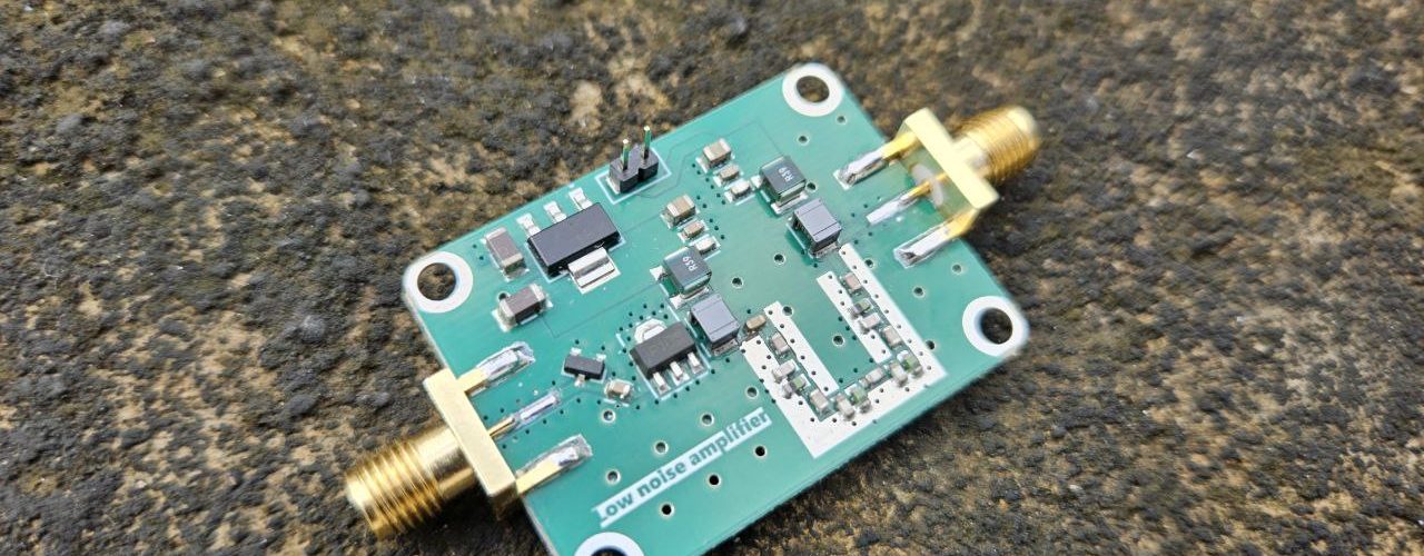
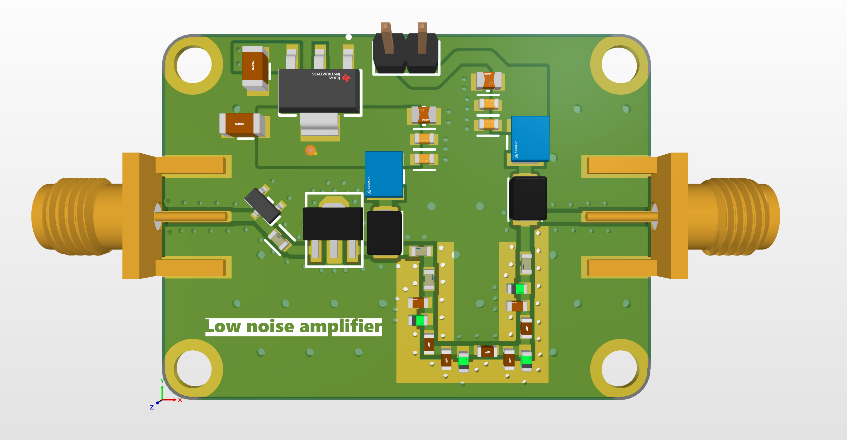
I got the design fabricated through JLCPCB. This is the first time I used their PCB assembly service. I found the soldering to be of very good quality. It took about a week for JLCPCB to get everything ready for shipment through registered post. Another 7 days and the package was at my doorstep.
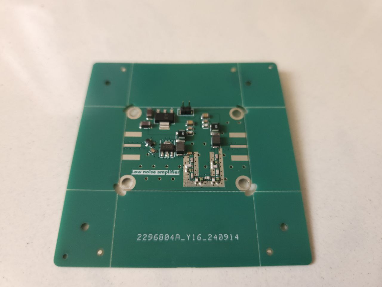
The boards came panelized like shown above. I broke the excess paneling material and soldered the SMA connectors.
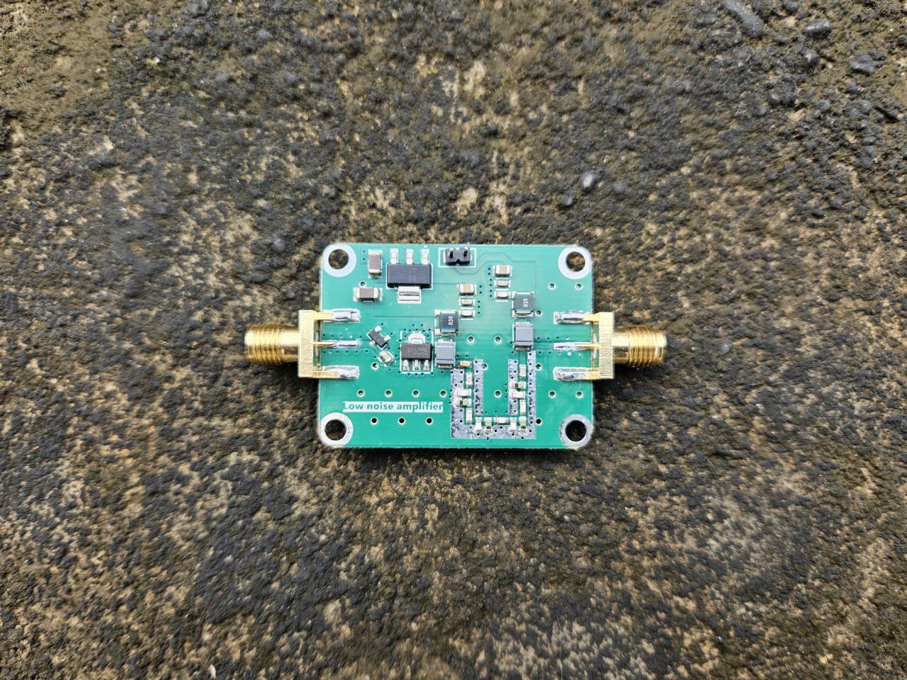
The boards looked wonderful but looks aren’t the only thing we see when it comes to PCB. We need to test it!
What do you think about this design? Let me know in the comments below. Thank you for reading my blog.
The part 2 is up and you can read it at the link below.
Part 2
On public demand, I am releasing the design and fabrication files for everyone. Contact me for blank boards, they will be available in second half of December.
Be careful joining ground pours across filter elements. It can cause signals to leak along the ground pour before reaching the ground plane through the vias. Also using ultra high Q porcelain caps from companies like ATC or Johanson will help get a tad more gain.
Thanks for the tip.
High Q components will definitely help improve the insertion loss.
I will definitely keep the consider the ground pour tip in future designs.
Hi there! Thanks for the reply. I understand component selection for Bias-T, I was more refering to the three capacitors C3/C5/C7… What purpose they serve and how you selected the values. Are these capacitors similar to “bulk decoupling” or are they an additional stage of RF filtering?
Hello! I am making a similar circuit in Altium Designer. Can you please tell me what is the purpose of components C3, C5, C7 and L1 (and mirrored on the other Bias T)? How did you select these values? Thanks!
Please read the Bias Tee section in the article. I explained the whole thing including the part on how to select these values. Let me know if you need more clarity on this.
Hi there! Thanks for the reply. I understand component selection for Bias-T, I was more refering to the three capacitors C3/C5/C7… What purpose they serve and how you selected the values. Are these capacitors similar to “bulk decoupling” or are they an additional stage of RF filtering?
I selected them just like we select normal decoupling caps.
Large one for low frequency, middle one for slightly higher frequency and the smallest cap for highest frequency we want to decouple from the power line.
Similarly the inductors are chosen. The big one for lower frequency bands, the smaller inductor works well for higher frequency bands. Although this circuit has a bandpass filter in vhf band, so there isn’t a very strong need for such robust filtering on bias tee. But more the better.
Ok, I understand, thanks for your help. One final question. I see you have “removed” the solder mask in a band around the 50ohm RF trace. So the copper is exposed. Does that have any technical reason?
The only reason I removed a part of solder mask around the filter is because it will allow me to solder additional passive components around that area if I ever need to modify the filter.
You may leave the solder mask untouched and it would not matter at all.
Happy to answer any question you may have.
Ok that makes a lot of sense 🙂 Did you consider any regulators other than TLV1117-3.3? I see its recommended minimum input voltage is 4.7V… My intention is to use this LNA design with a hack rf SDR, which has its bias-T operating at 3.3v (i.e. considerably lower than 4.7V)…
I did not but you could consider using the adjustable version of the regulator in your design. On the other hand you can also completely bypass the regulator.
hello brother, Im a college student designing an RF project…………. um this amplifier is needed alot i mean thank you so much, can we get in touch on instagram or facebook ??
Let me know your questions in the comment and I will be happy to help you.
thank you so much !!! , how to design the amplifier circuit and simulate it online to show to my professor which tools should I use ? thank you so much for your efforts !!!!
I am designing an LNA based on the PSA4-5043+, but I have been researching for some time because it is necessary to extract the DC signal from the line, place a decoupling capacitor and then reintroduce it, it should be noted that I am designing it to be powered only by BIAS T
I hope this article helped you with your project. I have demonstrated the exact thing here. Let me know if you any difficulty in designing your LNA
I have designed it by connecting the output of the PSA4-5043+ directly to the SMA connector, to be powered by BIAS, as I have read there should not be any problem.
Great project! Designing your own LNA with bias tee and bandpass filtering is a smart move—especially for SDR and radio astronomy. The PGA-103+ is an excellent choice for low noise and high linearit
Your circuit board design is exactly what I have been searching for. Are blank boards available, or is the artwork available so I can produce my own? I am interested in adapting your design for the 222MHz band as well as producing one for the 2m band.
Thanks Dave, The blanks aren’t available at the moment. All are sold out. But I can share the gerbers with you over email. Please check your email.
Great article, this is exactly what I have been looking for as well. Any plans to make the gerbers available more generally, maybe via github or to create a new batch of boards that we can purchase?
The gerbers are uploaded. Please check the end of the post for the link to download them.
Dear , Mini Circuits recommends placing an RLC network on the input pin 1 to prevent instability. LOW FREQUENCY STABILIZATION CIRCUIT: 330pf + 150r + 620nH…
Can you insert it into the gerber file ?…Sandro