
Constructing an X-Band power amplifier with FMM5061VF
[s2If current_user_can(access_s2member_level1)]
As we go up in the frequency range, things start getting tricky. The discretely available capacitors start to behave like inductors. On the other hand, even a couple of millimetre long length of wire offers significant inductive reactance to change circuit behaviour. In short, everything has to be accounted for as we go higher on the frequency scale. My experience constructing this little X-band power amplifier has taught me new things related to microwave frequencies. In this post, I will share the entire process in constructing the FMM5061VF amplifier so that you can replicate this design for yourself.
The device
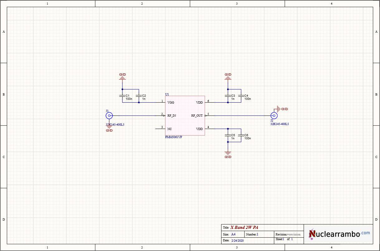
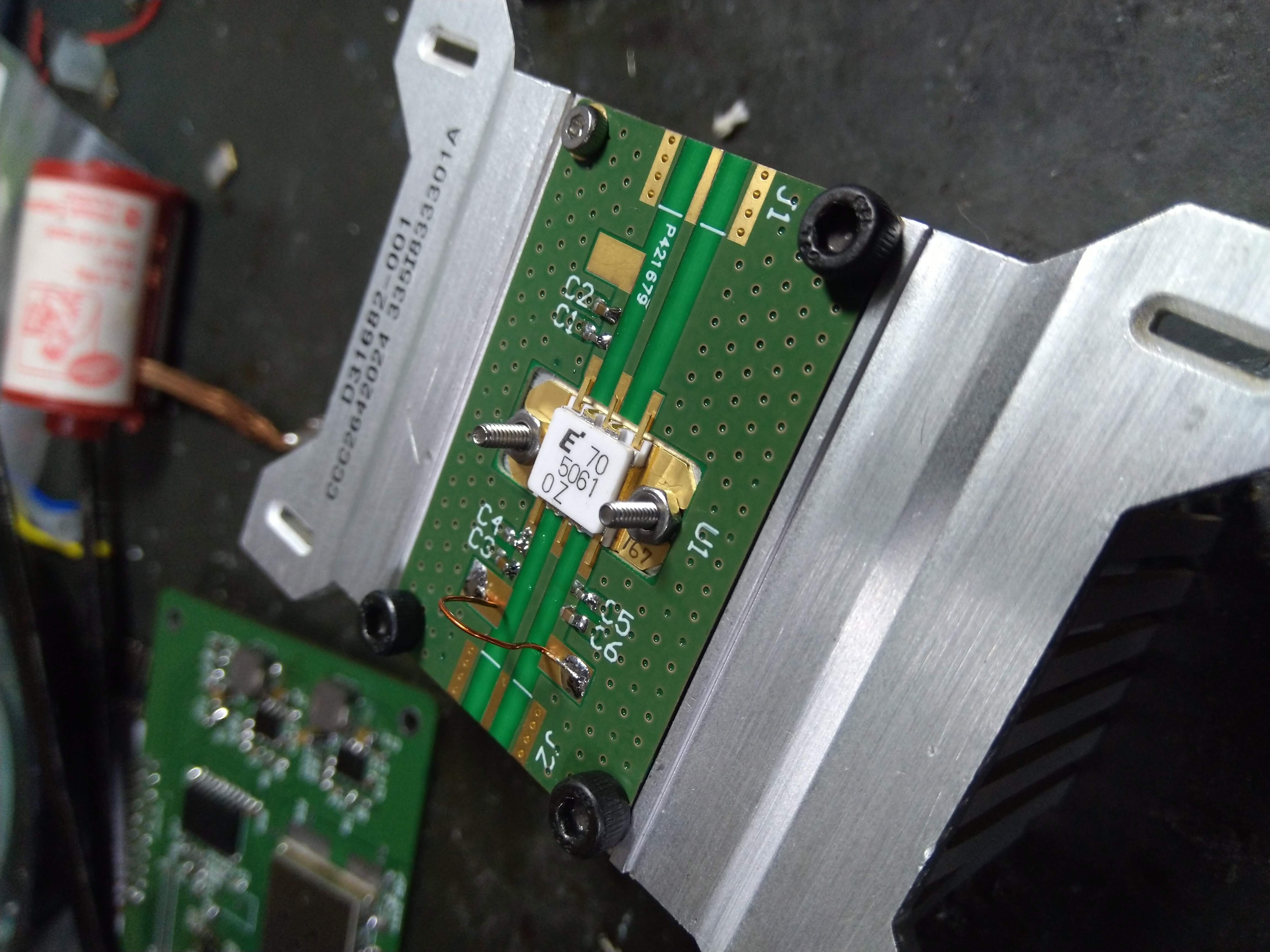
A couple of years ago I purchased two FMM5061VF amplifiers rated to deliver a maximum of 2W output power at 10GHz. It’s a GaAs device with three cascading structures inside that gradually add power to the input signal before finally delivering it. Based on the datasheet, it can add a gain of 24dB. We need to apply -5V to the gate supply input and up to +6V at the drain supply. You can always go higher on the drain side, all the way to 10V before creating any magic smoke. Fortunately, the FMM5061VF is internally matched to \(50\Omega\). That way, we simply need to design transmission lines that are well matched.
Designing the PCB
From my experience and based on comments from those with more experience, FR4 laminate will simply destroy the true performance of our amplifier. Therefore, it was clear that I will need to look for something else. The most common are Rogers laminates but they cost a lot. A slightly less expensive laminate with equivalent performance comes from Isola. My local PCB fab house offered Itera-MT 3.5 as one of their standard laminates to choose from. I went with the Itera-MT 3.5 laminate. It offers a \(tan\delta\) of 0.0032 at 10GHz as compared to a \(tan\delta\) of 0.0037 that the RO4350B offers at the same frequency.
Finally, I had made up my mind on using the Itera MT 3.5 substrate. The number 3.5 indicates the dielectric constant of the substrate. Creating the schematic was quite straight forward. The datasheet provided sufficient information to create the schematic which you can see below.
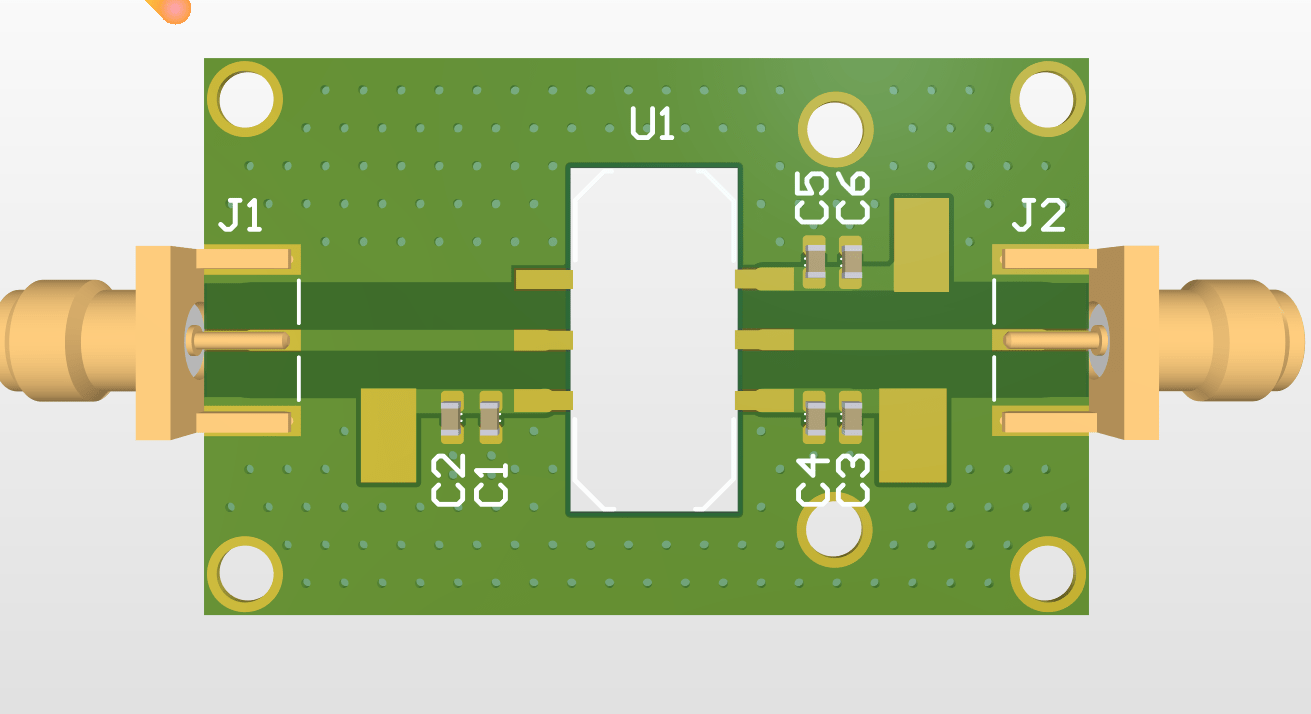
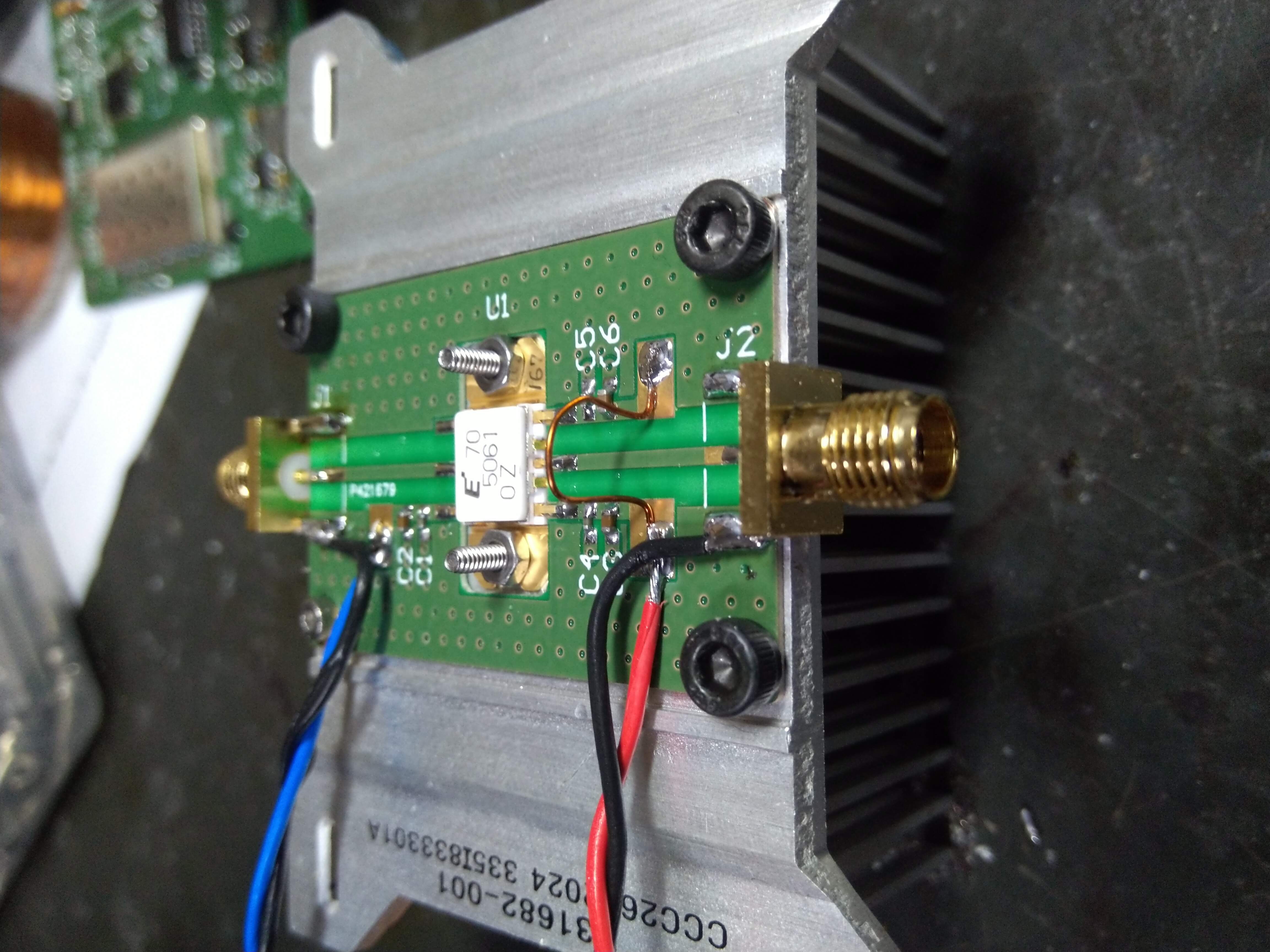
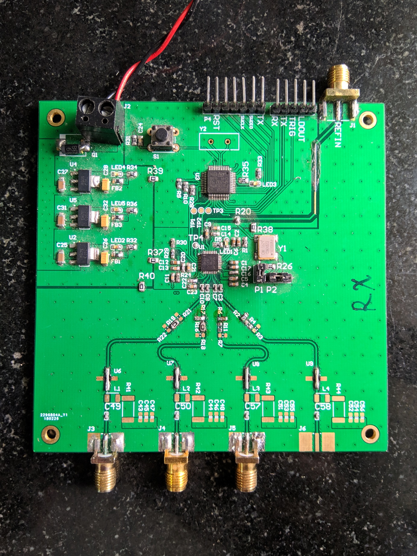
Creating the PCB wasn’t too difficult either. The amplifier requires power delivery from two pins. In between the two comes the RF output. Routing power underneath the RF isn’t a very good idea. So, the natural choice was to go overhead with a tiny piece of wire that does not interfere with the transmission line.
Troubleshooting
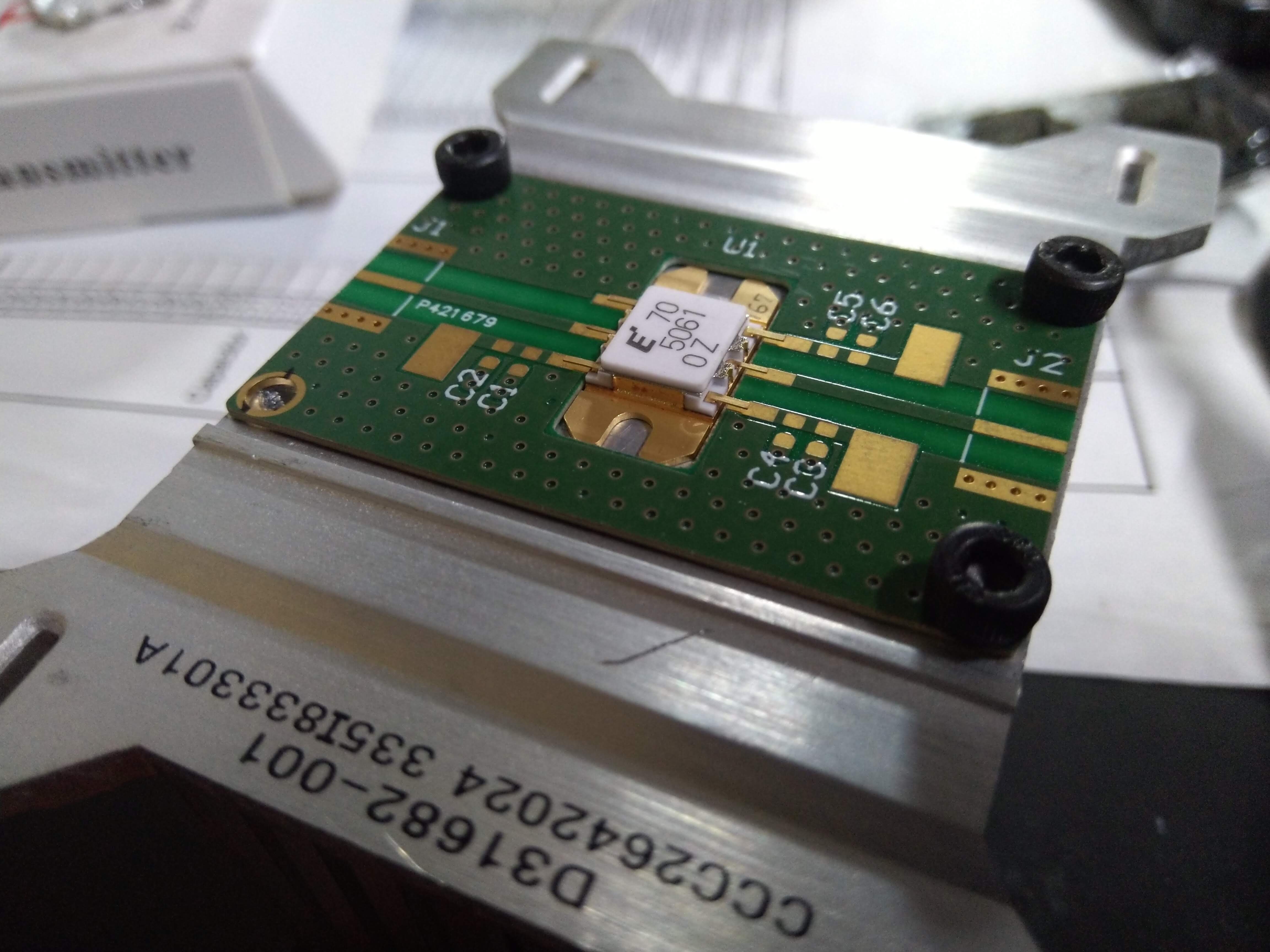
If you observe the PCB carefully, I forgot to remove the solder mask from the transmission lines. That isn’t a huge problem pertaining to the mask. The serious issue was the solder mask on the bottom side of the board which comes in contact with the mounting surface.
FMM5061VF gets its ground reference through its thermal pad. The thermal pad which is also its ground pad needs to be tightly placed on a flat metal body. Correspondingly, the PCB should also get the ground reference from the same body where the device is attached. My mistake in not getting rid of the solder mask from the bottom layer prevented proper ground contact. As a result, the amplifier started oscillating. Fortunately, the device did not get damaged.
Once I realized my mistake, I used sandpaper and brushed the solder mask from the bottom layer and re-attached it to the heat sink
Lesson learnt!
Like I said earlier, this setup started to oscillate and required repair.
After I cleared up the solder mask from the bottom layer, I re-attached it and tested it once again. The oscillations were still there except that this time the frequency of oscillation was around 11.5GHz. Now, I started thinking about various reasons that can cause oscillations in an amplifier. One of them was a bad output match resulting in reflections and as a result, feedback to cause oscillations. Another reason being, the ground plane of the PCB was still not evenly attached to the heat sink.
Upon carefully pressing the PCB with a plastic pen at various spots, I found the oscillations either changed their frequency or completely stopped. Finally, I found a sweet spot! Pressing hard on that spot stopped all oscillations. Now, I knew that the ground plane required proper contact. I quickly drilled a hole and tapped it for inserting a 3mm screw. That should attach the ground sufficiently well.
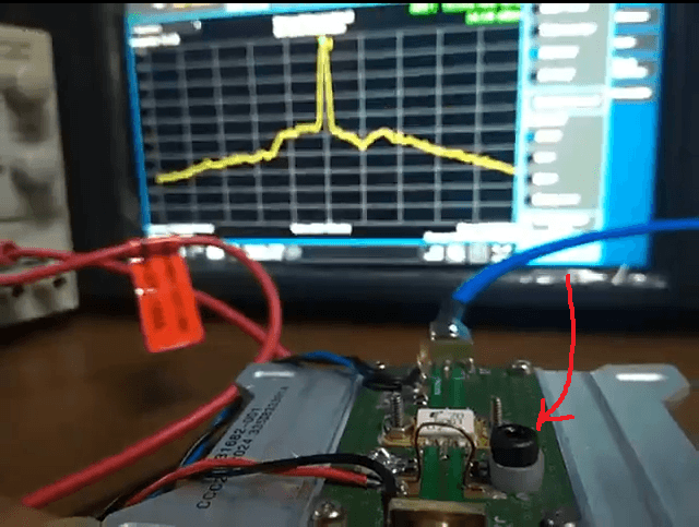
Lesson learnt that as you go up in the frequency range, the ground contact needs to be close to perfect. A millimetre of cavity here and there can make or break your circuit. Had it been a higher power amplifier, I might be possibly looking at several hundred dollars up in smoke!
Putting a wire over the transmission line orthogonal to it should be quite safe as it does not interfere with the EM fields around the line. May be, looping it too close to the trace might have changed the impedance a bit but compared to the wavelength, mine seems to be sufficiently away.
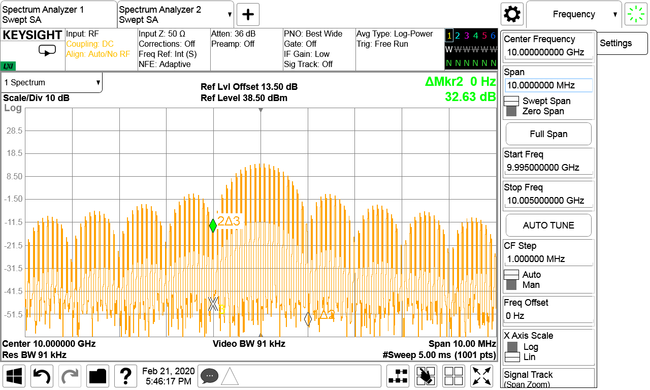
Test results
The test setup consisted of an RF source, spectrum analyzer and a nice little power supply. Obviously, we need two cables and an attenuator that can handle 2W of power.
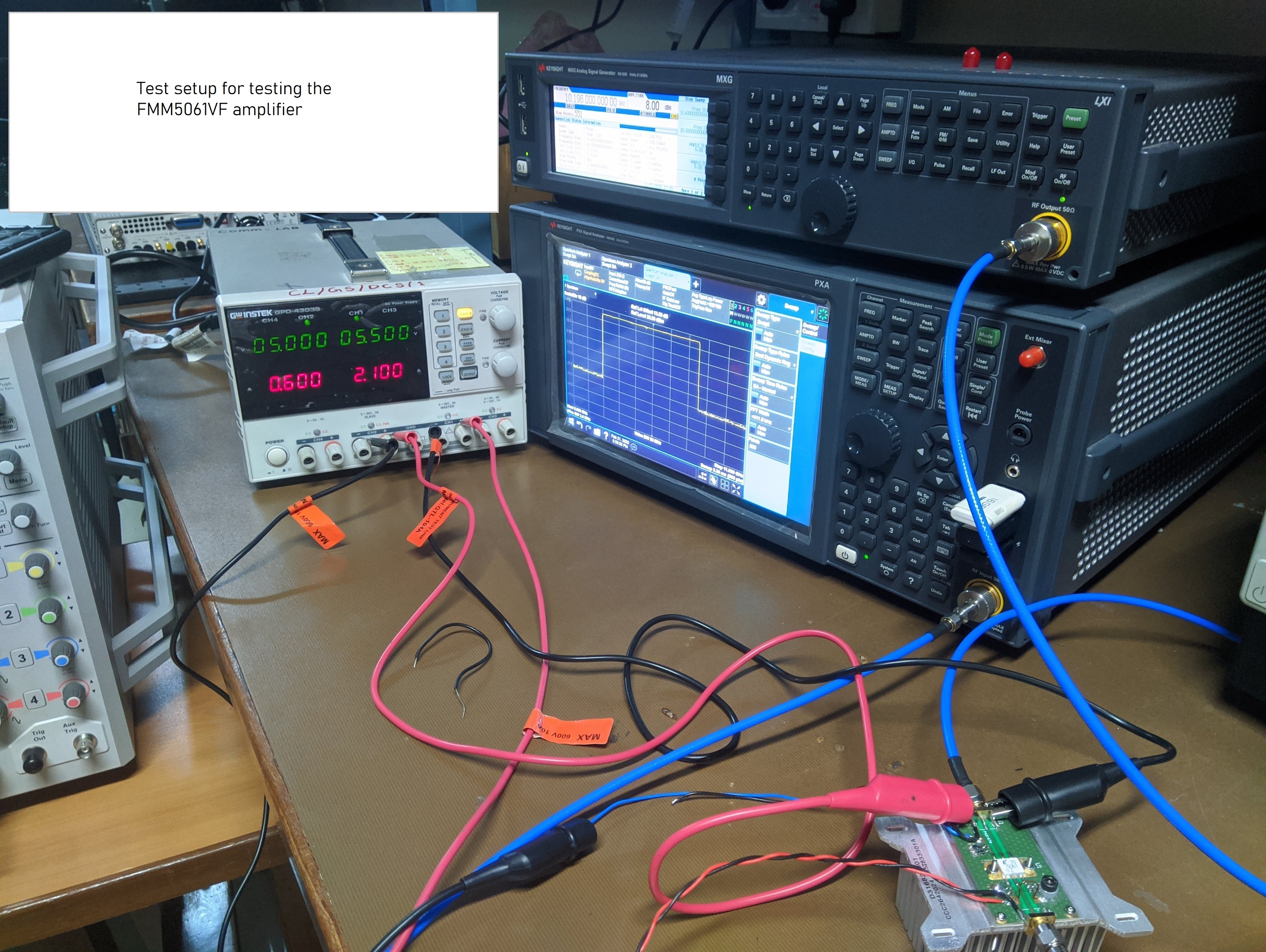
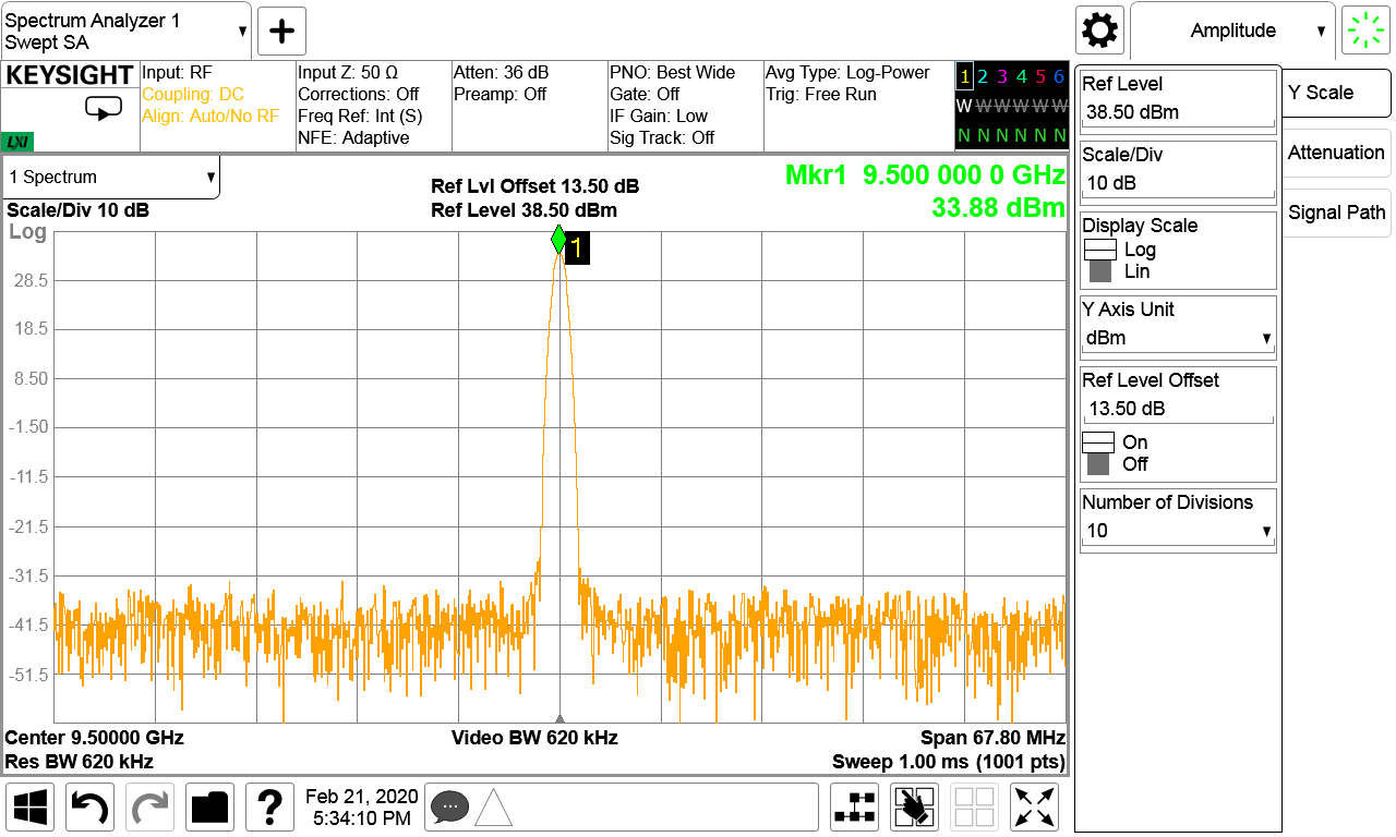
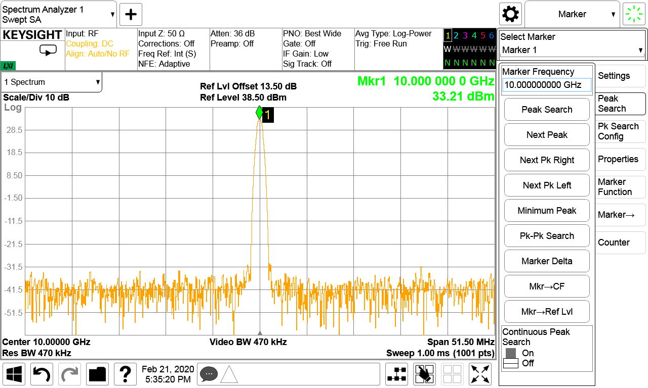
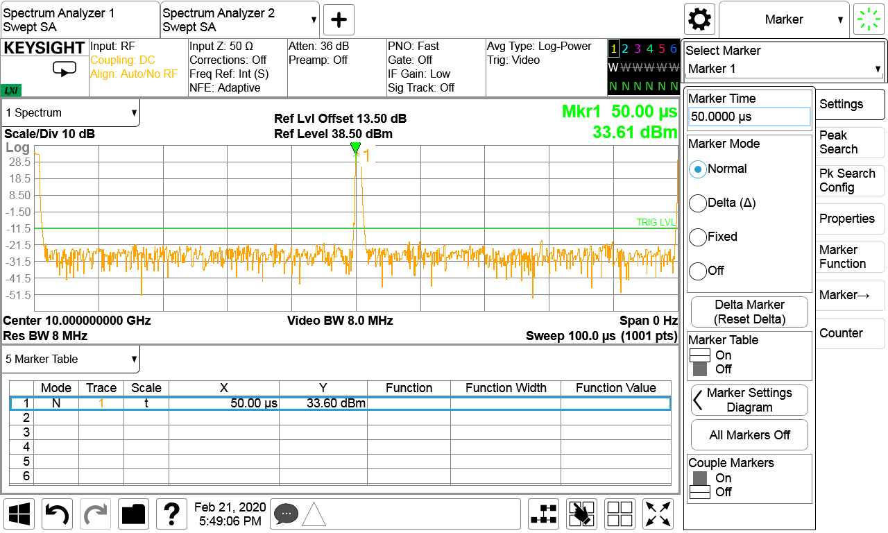
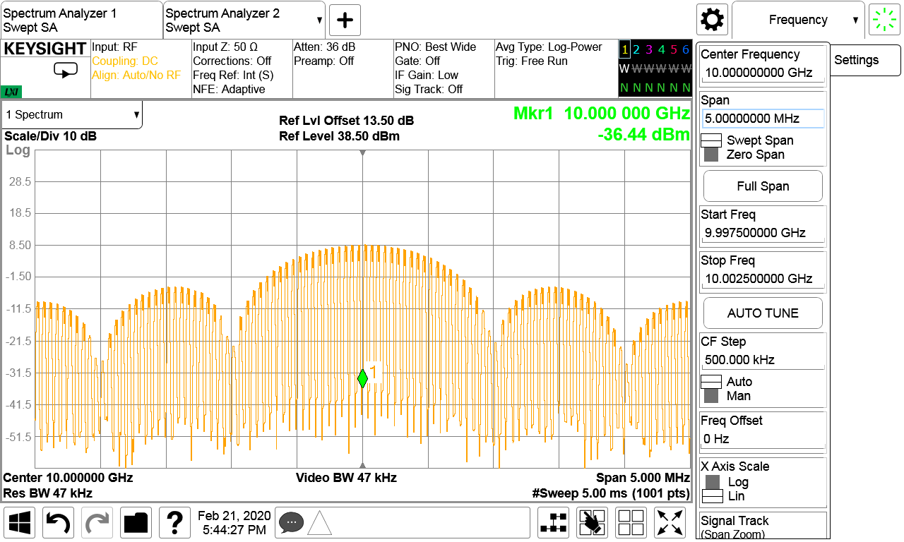
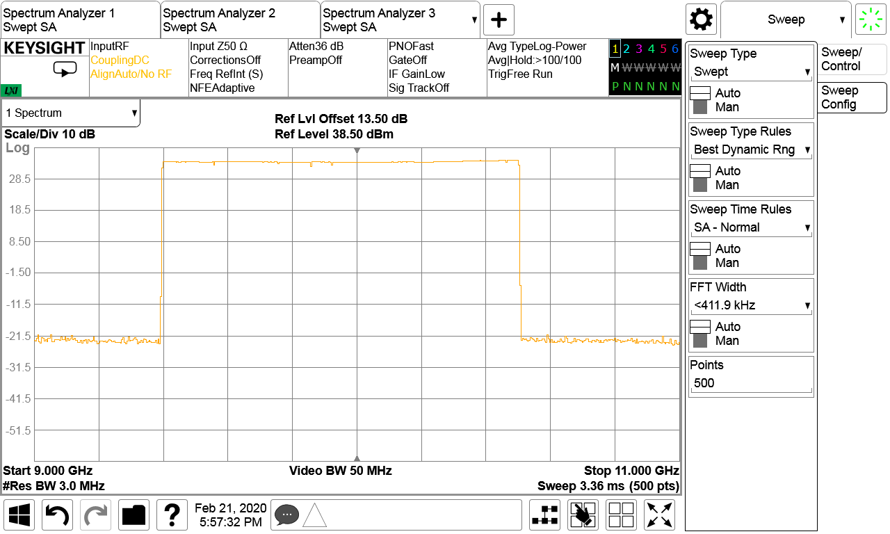
I was able to obtain a nice 33dB output and a specified gain of 24dB (maybe slightly less). Nevertheless, I was quite happy with the result. I am uploading all the raw results captured from the spectrum analyzer.
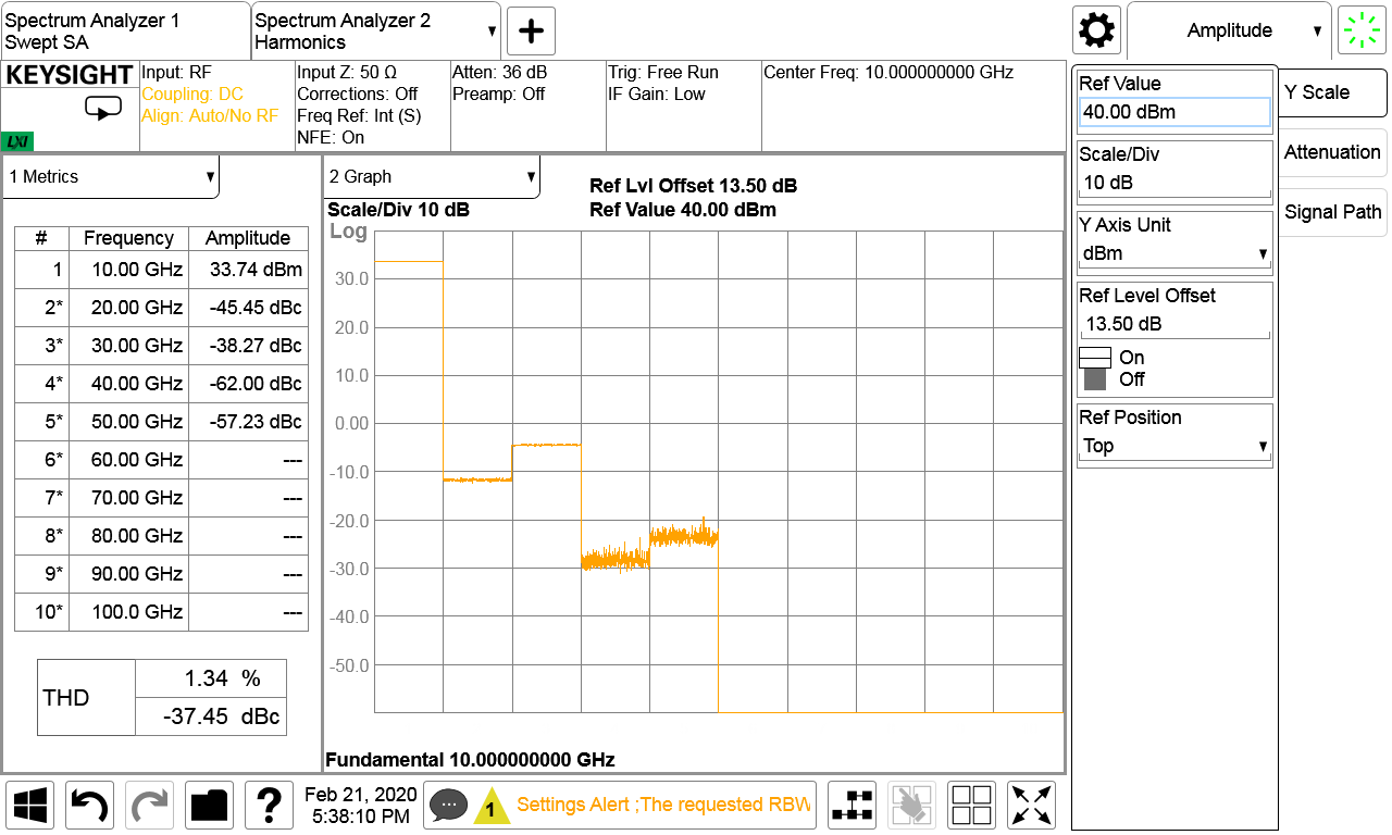
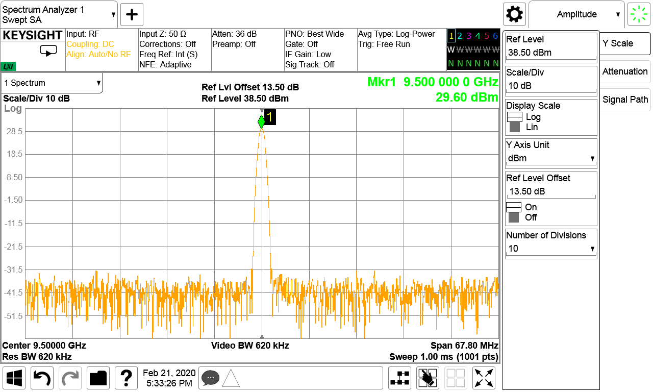
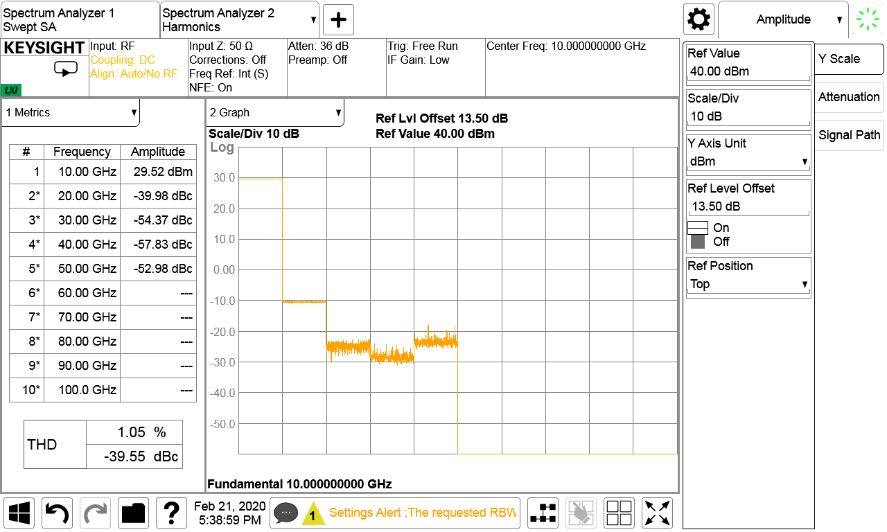
Now, once I was happy with the CW performance, I went ahead and provided a pulsed input to see how it responded to that. Practically, it is the gate voltage that also needs to be pulsed along with the RF input. However, I had no means to do that this time.
For those who spotted “Reference Offset” setting in the screenshots. I have attached a 10dB attenuator at the output of the power amplifier. Additionally, the cables offer 1.65dB at the input and output side each. Correspondingly, I have compensated for the loss by adjusting the reference offset.
Let me know if you wish to know more about this amplifier and I will be happy to answer.
Here are some legitimate links to the products from where you can buy this amplifier. Beware, there are a lot of fake ones on Aliexpress selling for less than $50. A legitimate device should cost in the range of $50 to $120. I got mine from an eBay seller from Greece and it cost me $99 per amp. Apparently, he doesn’t seem to be selling those anymore.
Amazon
Aliexpress
[/s2If]
[s2If !is_user_logged_in()]
The content in this post is restricted for registered LEVEL 1+ donor members only. Please consider signing up for level 1 donor access. If you are already registered, consider signing in.
REGISTER | SIGN IN
[/s2If]
[s2If is_user_logged_in()]
[s2If current_user_is(s2member_level0)]
This content is out of bounds for general users. Due to the nature of content, we require you to support us by donating. Please consider clicking the following link and donate.
[s2Member-PayPal-Button level=”1″ ccaps=”” desc=”Bronze Member / Description and pricing details here.” ps=”paypal” lc=”” cc=”USD” dg=”0″ ns=”1″ custom=”nuclearrambo.com” ta=”0″ tp=”0″ tt=”D” ra=”0.01″ rp=”1″ rt=”M” rr=”1″ rrt=”” rra=”1″ image=”default” output=”button” /]
[/s2If]

Hi sir, i have a question abut this,amplifier, do you have impedance of gate and drain pin? And whats best vgg fir this amplifier? Thanks
Hello.
I am from Ukraine.
I have developed Digital Antenna Arrays radar proototype and I need now at least 2W power amplifier for 10…12Ghz band. Can you propose ready to use device or can you recommend any link with peoples interested in this? ? Thank you. Best regards, Viktor.