Seeed Fusion PCB fabrication review 2022
I reviewed JLCPCB PCB fabrication service a few years ago. Since then a lot has changed. There have been stories, both good and bad about JLCPCB. You can read the comments on that post. For today, we will be looking at the Seeed Fusion PCB fabrication service. I will try to keep this review short and to the point. Seeed did sponsor the PCB fabrication for this review, but that won’t affect my view about them anyway.
Preparing your PCB
Seeed Fusion can fabricate up to 6 layers according to their ordering page. For a higher number of layers, they offer professional services that can be a bit costly for hobbyists.
When it comes to two-layer boards, PCB thickness options go from 0.6mm and 2.0mm with the standard surface finish options such as ENIG, HASL, etc. Fortunately, you can also have Matte Black finish on your PCB. Not everyone offers this solder mask finish, and Matte Black is one of my favourites. Unfortunately, Matte Black solder mask costs extra money whereas, all other colour options don’t.
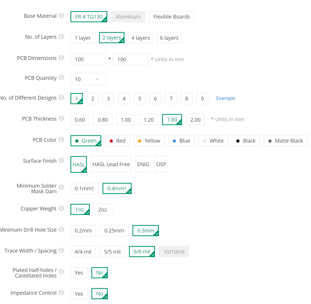
While going for a higher number of layers, sticking to their default board stack-up proves to be an economical choice. A custom stack-up costs a lot of extra money and quickly becomes unreasonable for a hobbyist unless you are into designing exotic RF circuits.
A standard stack-up for multi-layer PCBs can be found at this FAQ link.
In my case, I could only fabricate a 2 layer PCB within 100 x 100 mm. dimensions without blowing up too much money.
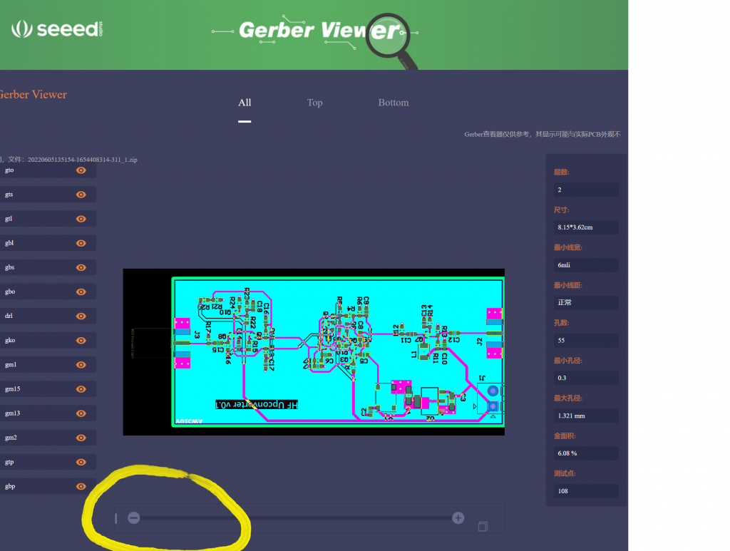
Apart from that, when you upload your gerbers you have the option to view your PCB in their gerber viewer. Unfortunately, the gerber viewer seems broken and doesn’t behave the way it’s supposed to.

A word about PCB assembly
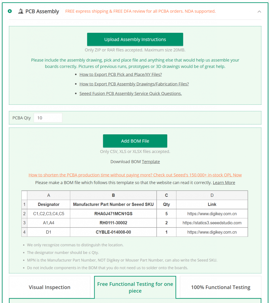
If you wish to get your PCB assembled with them, you will need to ensure that you also upload the BOM along with your gerbers. When opting for PCBA, the exact price estimate comes a bit later, depending on the stock. Additionally, Seeed Fusion also offers basic PCB functional testing upon assembly. Compared to others offering similar services, the Seeed Service was on a higher side. I cannot comment more on this since, I only went with the PCB fabrication and dropped my assembly plans after seeing the cost. For a company doing this for commercial purpose, the pricing is super competitive. On the other hand, a hobbyist with a minimal budget like me may prefer to assemble the PCB independently.
Tracking your order
I successfully placed my order with Seeed Fusion and the clock started. They have a system that lets you track every step of fabrication right from design review to dispatch.
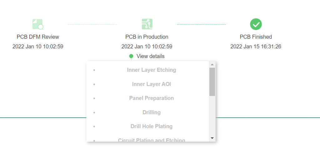
It took about five days for the fabrication to be complete and dispatch. In another week the PCBs arrived through DHL.
Fabrication review
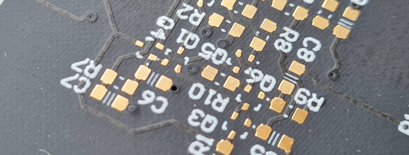
Watching your PCBs up-close is the most exciting part of the entire process. I am sure many of you would agree with me on this. Looking at your creation closely and reviewing in your head about how it’s all come out in reality is an important step. The PCBs came packed in a nice yellow envelope with a small plastic bag inside containing the boards.
Fabrication looked to be quite fine and done well.
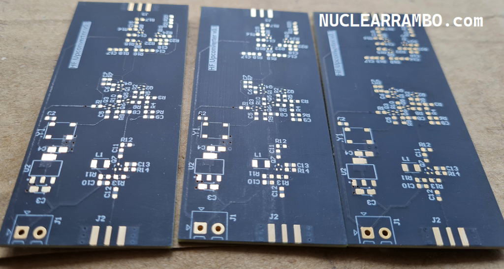
The matte black looks quite acceptable to me. Apart from that, I did not find any connectivity or short circuit issue in the boards indicating a flawless fabrication. I deliberately kept the boards unsoldered for over 5 months to test the ENIG process. Often times, the cheap fabrication houses use really poor gold plating that gets corroded over time. Apparently, Seeed Fusion PCB ENIG process did not corrode and I am quite happy about it.
Copper surface finish
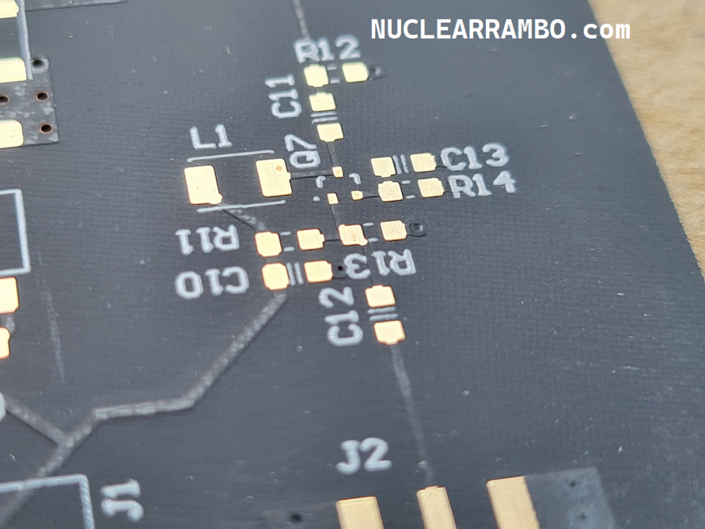
Closer observation reveals a nice slanted weave pattern. Those doing high speed design and RF design know the significance of a slanted weave pattern.
A slanted weave pattern often helps in reducing minor impedance variations. Weave pattern causes very tiny variations in the capacitance as the trace goes across the PCB. Being a weave of fibers, there are periodic distances where the distance between the trace and dielectric reduces and the capacitance increases. Consequently, there are points where the capacitance reduces as a result of increased distance. Practically, this variation in distance is only a few micrometers and even this becomes significant at higher frequencies or high data rates. Apparently, a slanted weave pattern helps reduces such variations, thereby reducing the reflections arising due to this effect.
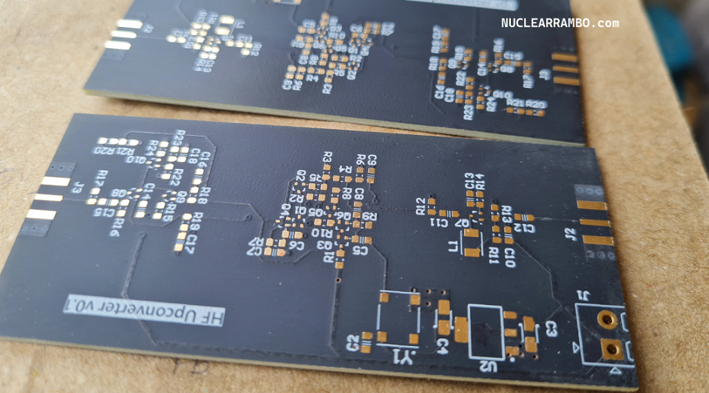
The text overlay or the silkscreen print has come out really clean and tidy. There are no breaks or instances of illegible text anywhere on the board. A nice clean text always makes me happy because it kind of adds to the beauty of the PCB. Oftentimes, you spend several hours fixing the overlapping silkscreen only to make the board look beautiful. It can get saddening when your silkscreen gets printed poorly, something in which you have put significant time. Seeed Fusion did not disappoint.
Conclusion
After covid, prices are jacked up almost everywhere as compared to the prices in the pre-covid times. Yet, Seeed Fusion PCB fabrication remains quite affordable for simple 2-4 layer designs with no special requirements. I had a pretty good experience when Seeed Fusion and I might fabricate more boards in the future when need arises. For less than 50$, I was able to get 10 boards fabricated from them with ENIG finish. It would have been even cheaper had I gone for HASL and glossy black soldermask,

Voice of the people