
Reviewing the new NanoVNA v2 (SAA-2) – Part 1
The first version of NanoVNA became an instant hit for very obvious reasons. First, it was offering stunning performance. Second, a super low price which brought VNA into the hands of those who would have never thought of owning one. Third, the open source nature of the project resulting in excellent variations of the device, each one better than the previous iteration. Soon after that, NanoVNA 2 came into development and later showed up on a couple of online stores by the month of March. The new NanoVNA v2 extends the upper frequency range all the way up to 3GHz. Although it uses 4.4GHz capable exciter, the reflection bridge degrades beyond 3GHz.
I will be reviewing the very first Tindie version of the NanoVNA v2 which comes with no accessories. At the time of writing this article, a second production batch is being sold on Tindie and Alibaba where customers can choose to include essential accessories!
First impressions
I purchased the NanoVNA 2 as soon as the first batch of production was out. It sold for $53 a unit and I purchased 2 of them before the stock ran dry. Soon after purchase, it was shipped, it reached one of the Chinese airports and there was lockdown announced due to the pandemic. After nearly 3 months, patience finally paid off and the package was delivered. As expected, the unit came with no accessories unlike the NanoVNA v1 which came with the cal-kit and cables.
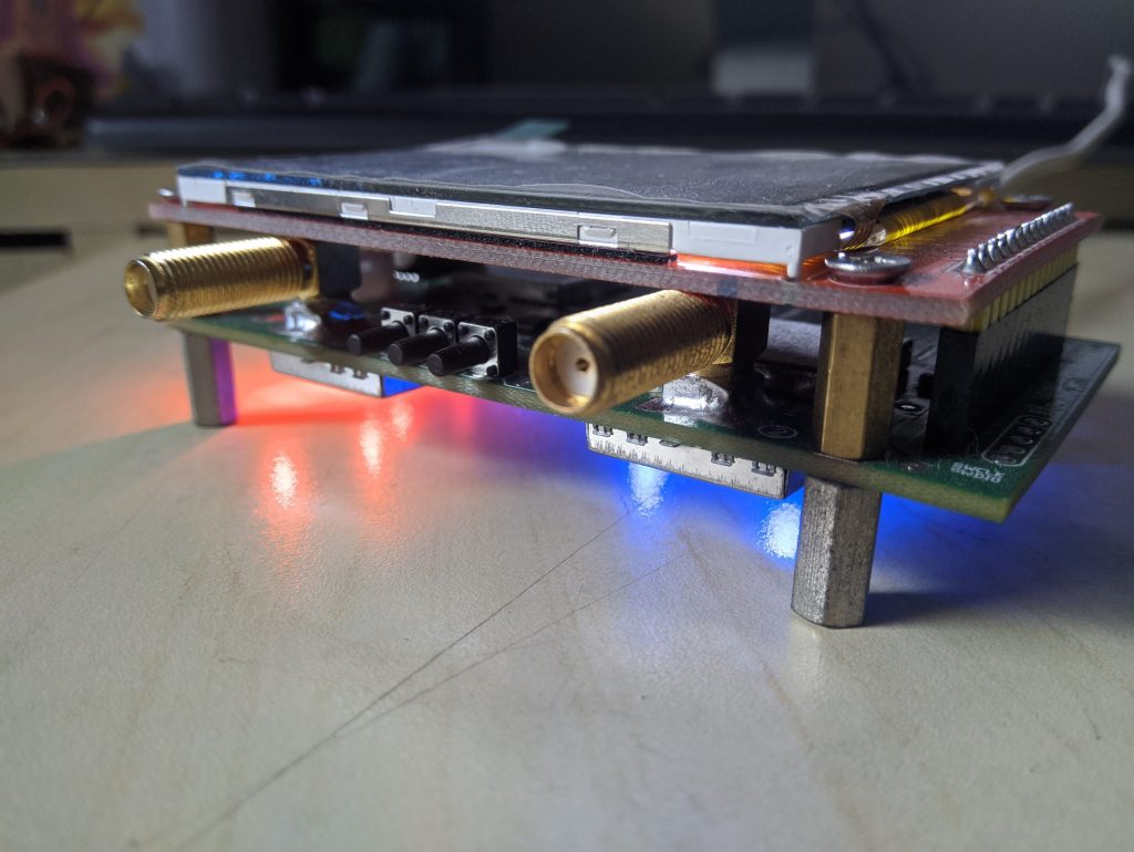
Exposed bottom part
The bottom part of the PCB sits directly exposed. It worried me a bit considering there was no stand off and the components touch the surface wherever I keep it. The first thing I did was to attach 4 PCB stand offs to prevent any mishaps in case I happened to place it on metallic surface.
USB connection
The design remains unchanged except you now get all the essential accessories including battery and a clamshell case. My unit had no battery because that’s how it was being sold back when it came out. Fortunately, it runs well over USB power. Although, there’s a major change here. The NanoVNA v2 comes with an old micro USB port unlike the NanoVNA v1, which came with USB type C. The downgrade is a bit disappointing because a lot of us now have USB-C cables at our homes. I had to borrow a micro USB cable to power up this unit.
Display
Sometime ago, we had the nanoVNA H4 come out sporting a larger 4 inch LCD display. A lot of us had hoped that the NanoVNA v2 would ship with a larger screen but that did not happen. On the contrary, NanoVNA v2 comes with a 2.8 inch display. Although, the developers claim that certain 4 inch displays would work right off the bat without any firmware modifications. If you do not want to mess around with different displays, you should simply wait a little longer because larger display is definitely coming out soon.
Accessories confusion
Speaking about the battery once again. HCXQS, the company that sells these units wanted to keep the price as low as possible. So, they cut costs on the battery, clamshell casing, the cables and also the calibration kit. After a while, Hugen who was mainly responsible for the earlier NanoVNA v1 came with his own product along and that included all the aforementioned accessories. In short, if you buy NanoVNA v2 today you will be able to get the essential accessories in the box. As a result, the price has also jumped up a little and if you purchase all the accessories it maxes out at $70 a unit. You can still opt-out and get the very basic model for $53 and probably build your own case and cal-kit.
Remember the delicate jog-wheel on the NanoVNA v1? Fortunately, that’s gone and replaced with 3 push button switches. The SMA connectors are longer and pop out sufficiently in case you want to insert it into a case. Another big change is sufficient amount of shielding over critical RF components to improve the noise floor and interference.
The electronics inside NanoVNA v2
We will go over basic operation of the design and the changes made over the version 1.
PLL based exciter
The NanoVNA v1 is known to work all the way up to 1.5GHz. The excitation signal being generated using the harmonics of the Si5351 oscillator chip had its own limitations. Additionally, the board wasn’t designed to work all the way that high. We all know that the harmonics contain lower power than the fundamental tone. Additionally, the mixer chips weren’t meant to be used for frequencies that high either. So, we can get quite good dynamic range and low noise floor up to 300MHz, but then it degrades. In short, the first NanoVNA wasn’t designed to go that high.
In order to truly reach such high frequencies, several critical components are replaced with better parts. The first one being the excitation signal source. Instead of Si5351, the new design uses ADF4350. This PLL chip is capable of generating frequencies all the way up to 4.4GHz and it can switch frequency in less than 100us (if band select clock is increased). Nevertheless, this chip is great in terms of phase noise performance. Adding an ADF4351 would have been excellent considering it has even better phase noise and lower PFD spurs. An exactly pin identical chip MAX2870 can take our higher frequency range all the way to 6GHz. May be we can see this in a future version!
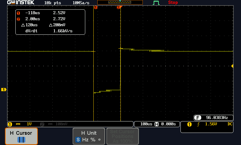
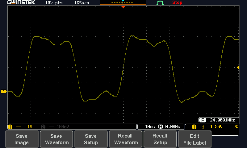
Here, we can see the lock time of the ADF4350 PLL. It is about 120us which is about right duration.
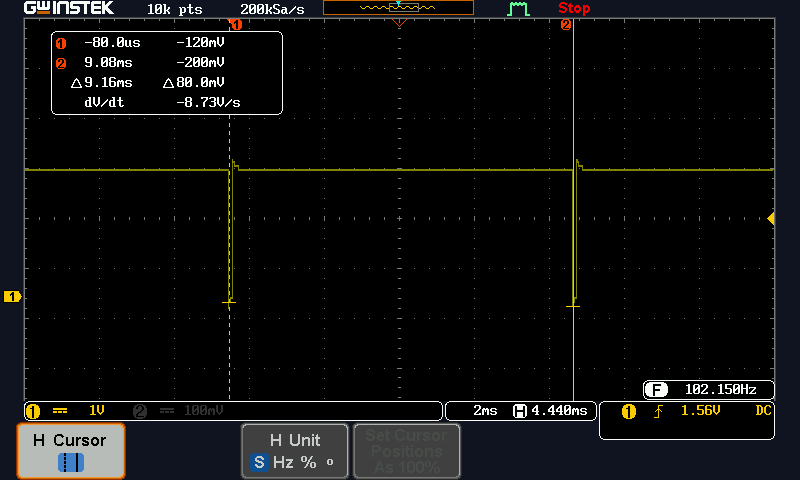
In the second image we can see the time between two frequency steps. Amounts to roughly 9-10ms which equals nearly 100Hz average. That’s right because the specified sweep rate is 100 points per second.
TX Path
The PLL chip doesn’t tune to frequencies below 137.5MHz. The Si5351 covers the low frequency band very well. Now, to switch between two excitation sources an RF switch MXD8641 comes into the picture. The switch has a rating up to 3GHz and gives a path loss of 0.4dB. Right after, the directional coupler attenuates the excitation signal by another 10dB. Furthermore, an on board electronic calibration circuit automatically calibrates the VNA up till the SMA connector. For this, we have another MXD8641 switch in the path.
RX Path
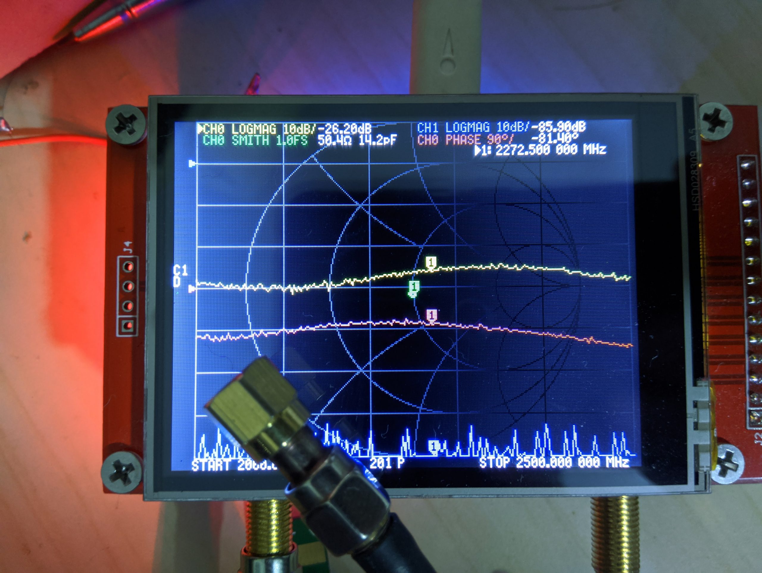
The circuit follows a similar design on the receiver side with two local oscillators. One for the high frequency, and another one for lower frequency. The directional coupler according to the schematic offers a coupling factor of -20dB. The reflected signal then passes through a bunch of switches and lands at the input port of the mixer. Analog devices AD8342 with average conversion gain of 3.5dB across its operating region. The mixer’s input P1dB stands at nearly +8dBm. Hooking up an active device is the only way you will ever exceed this limit. Try to use an attenuator while doing active measurements.
The GS8722C dual Operational amplifier works like a simple base band IF amplifier. An additional RF switch selects between two gain levels before being fed to the STM32 microcontroller. In fact, the NanoVNA v2 comes with GD32F103, a Chinese variant of the STM32 with a higher clock frequency. The ADC on the microcontroller samples the IF signal. Looking back at the NanoVNA v1, an audio codec chip did the sampling and had a higher dynamic range but limited by the sampling frequency. That’s the reason the NanoVNA v1 could not have higher IF frequency.
Instead of having two separate paths for the reference channel and RX channel, a bunch of switches route both the channels into the mixer and the software alternately samples the two signals. This happens to be one of the reasons that slows down sweep rate.
The reference oscillator
The NanoVNA v2 uses a 24MHz TCXO that drives the 74LVC2G04 dual inverter. This chip behaves like a clock buffer. The output of the inverter directly drives various other chips such as the MCU, 2x PLLs and 2x Si5351 oscillators. I haven’t done any phase noise measurement on the oscillator output and nor could I find the exact part number. I am assuming it isn’t a high precision part. Therefore, frequency stability may get affected greatly when the PLL generates outputs in the GHz range.
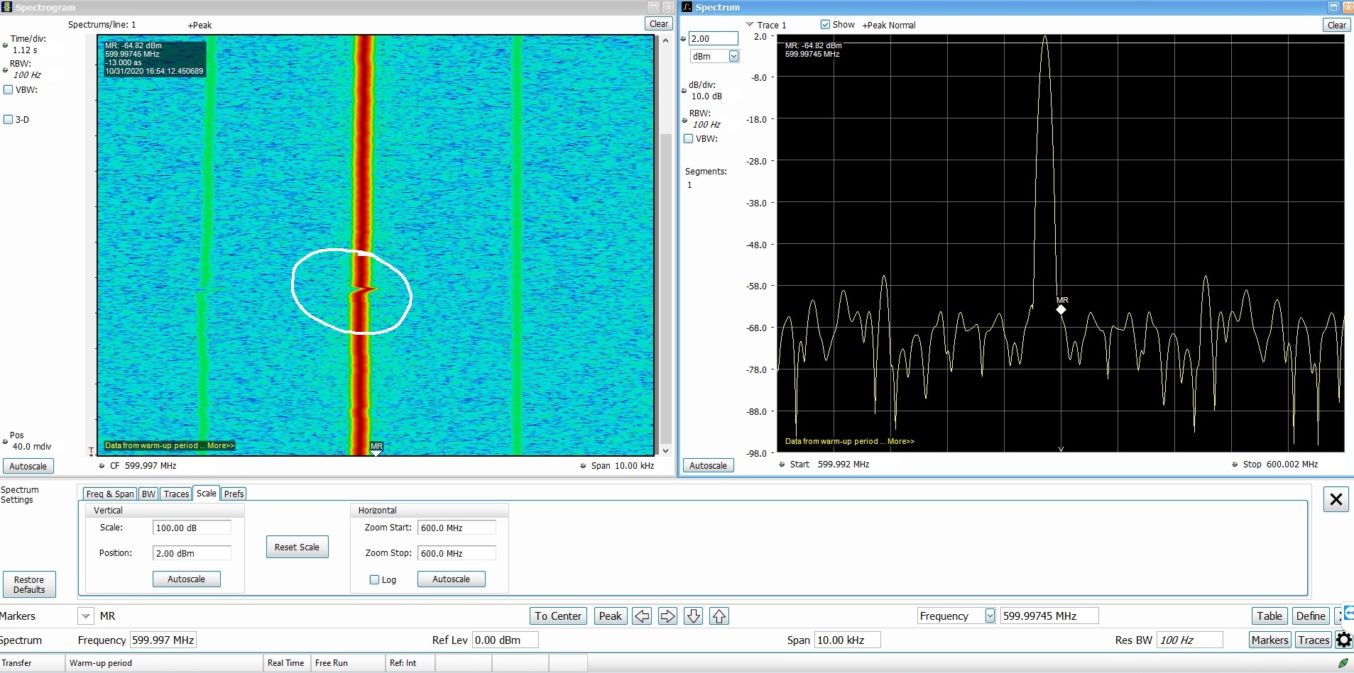
Considering the pandemic I do not have access to the tools that I need to do measurements to look at the spurs, emissions and cross talk between the two PLLs.
I wasn’t able to get the BOM for the NanoVNA2. Therefore, I am unable to verify whether the passive components used are capable of operating in the GHz range. Usually, passive components come with a rating for self resonance. Beyond their self resonating frequencies, inductors start behaving like capacitors and vice versa. If any of you readers could like to the latest BOM, I would be grateful.
Connectors
The NanoVNA v2 comes with right angled through hole SMA connectors. Such connectors have an upper limit in terms of frequency. In my opinion, the ideal candidate would have been 9mm edge mount connectors that work quite well all the way till 12GHz. The only way to know how good these are would be to procure it individually and measure it over a test PCB.
I will end the part 1 of the review here. In the part 2, I will actually carry out a few basic measurements and go through the software interface.

1 Response
[…] In the part 1, we reviewed the hardware aspects of the NanoVNA v2 SAA 2. Here, we will review the actual functionality of the device. […]