
EM simulation over a PCB designed by you
Doing electromagnetic simulations on your PCB layout can be a difficult task. The main reason being the tremendous effort required in porting your PCB layout data over to the 3D EM simulation software. Fortunately, new updates to the EM solver tools have made our work simpler. In this article, I designed a very basic co-planar waveguide and used AWR Design environment to conduct an electromagnetic simulation to test for its high frequency performance.
EM simulations prove to be quite helpful when designing layouts meant to work at high frequencies. In case of a co-planar waveguide, parameters such as the conductor gap and via distance play an important role especially at frequencies above 6GHz. In addition to that, the coax to PCB launch interface also plays a very crucial role in determining the overall performance of your design. We won’t be going too much into detail about RF design in this article. Instead, we will be focusing on the method with which you can send your layout from your primary design tool to the AWR design environment to do the EM simulation.
Generating the design
Altium Designer is my primary PCB layout tool. It could be something else for you but the method remains quite identical. I designed a very basic co-planar waveguide structure in Altium. The design has an edge mount SMA connector on each side of the co-planar waveguide. I calculated the waveguide geometry using the AWR Designer Environment’s TXLine utility as follows.
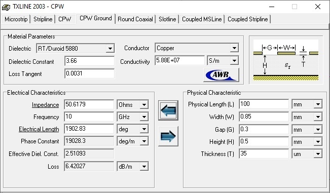
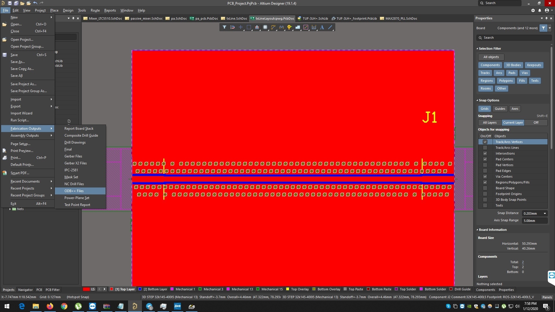
Using the parameters obtained from TXLine utility, I designed the layout in Altium. Further, I exported the odb++ outputs that you can see below.
Importing into AWR Design Environment
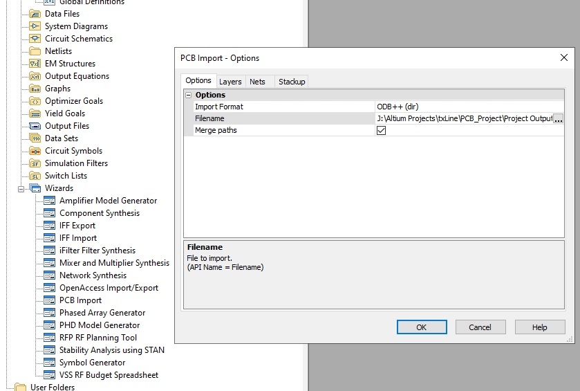
Importing layout files into EM simulators become a lot simpler over past few years. AWR Design environment directly accepts ODB++ files. We shall use this provision to move forward.
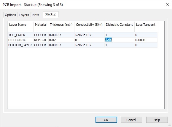
While you are at it, make sure to jump over to the Stackup tab in the window. We need to edit the PCB stackup to suit our design. In my case, I have a RO4350 laminate having 0.5mm thickness. As per the RO4350 datasheet, we need to consider the 3.66 dielectric constant.
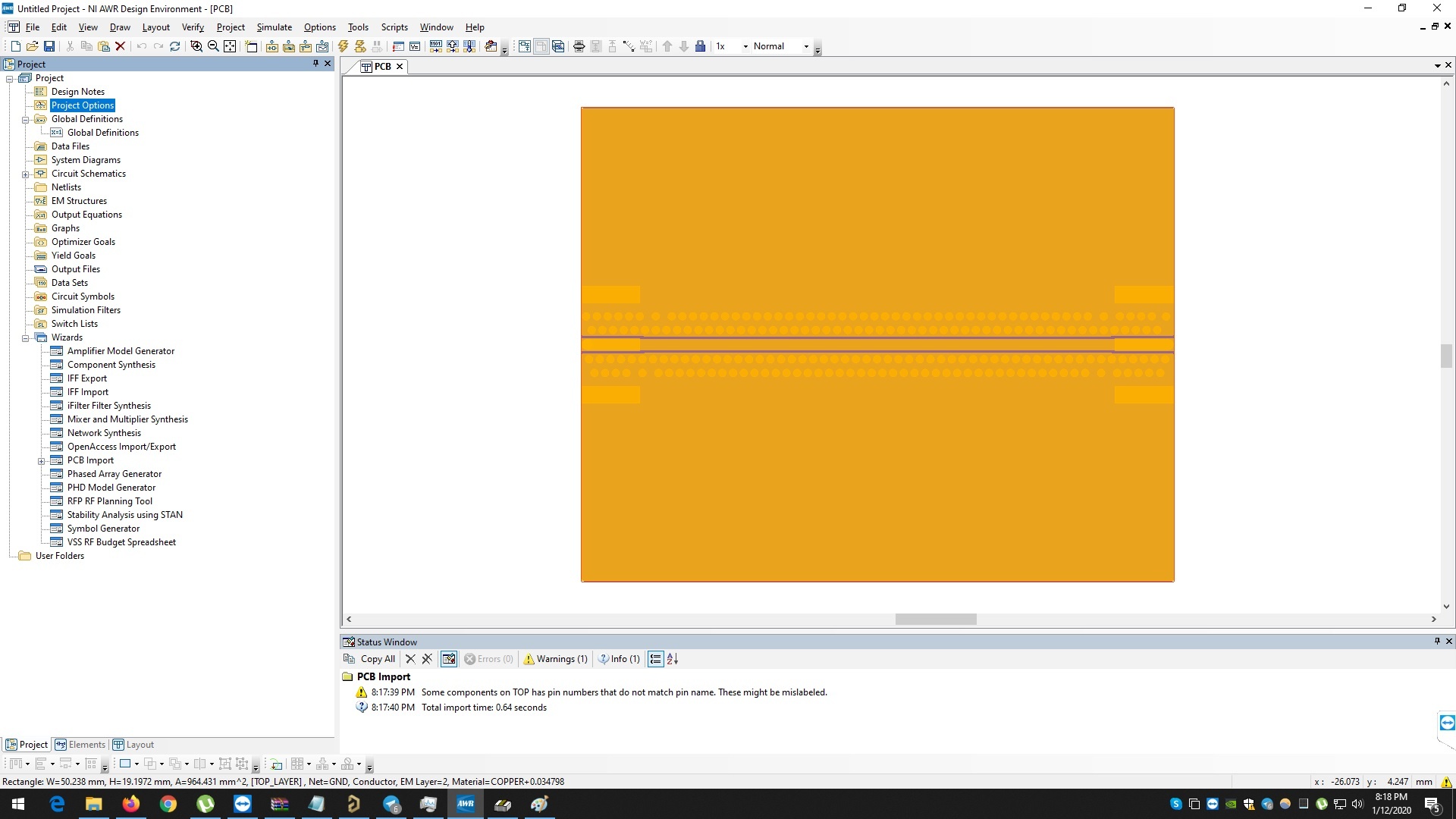
If everything goes right, you should be able to see an imported layout in your AWR window.
Setting up our EM simulation
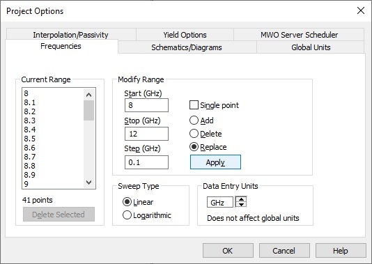
Now, we need to setup simulation parameters like excitation ports, output measurements and so on. Firstly, let us define the simulation frequency range by going into the Project Options > Start and Stop frequency.
Now, we need to convert our layout into an EM structure. Meshing and all sort of computations will finally occur on the EM structure. Select the entire layout by dragging your mouse over it. Once everything is selected, simply go to Layout > Copy to EM structure.
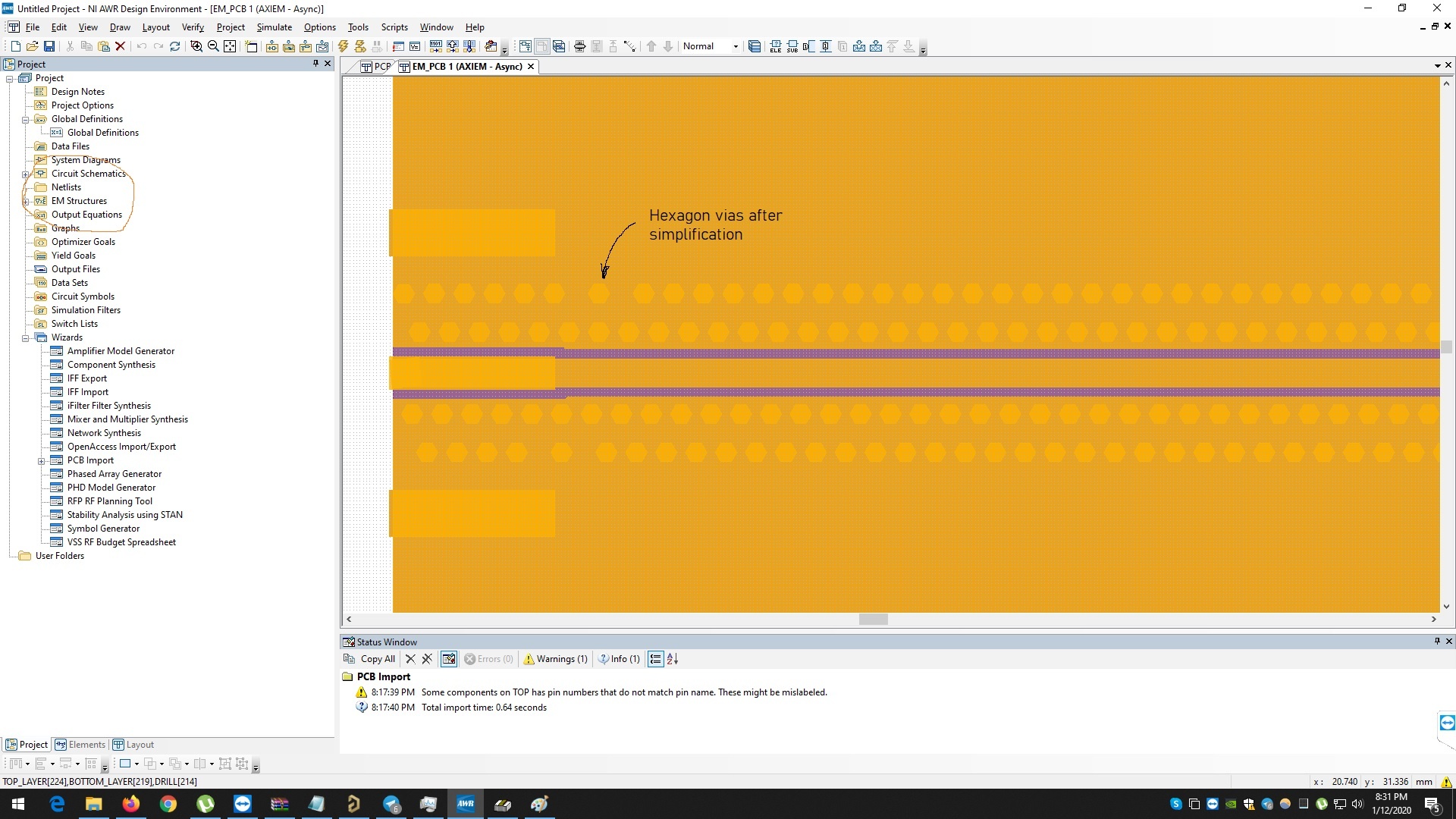
Doing so will result in a window that looks something like below. Simulating fine details in your layout will take ages. Instead, we simplify the model before jumping in. For example, circular vias can be converted into square or hexagons.
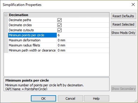
Curved traces need to be converted to traces with rectangular or sharp edges instead of curved ones. This helps simplifying the mesh complexity. At higher frequencies, the mesh is extremely fine and simplifying your EM structure greatly speeds your simulation time.
You can now view the 3D EM structure by right clicking on the EM Structures option in left sidebar and clicking on “View 3D…”.
Let us now add excitation ports by going to the file menu, Draw > Add edge port. Place your edge port on each end of the transmission line. With this, we are ready to move forward. Additionally, you can also edit the EM structure a little as per your requirements. I deleted certain unwanted overlapping pads and shorted the trace a little to align everything with each other.
We can now proceed to simulate our design.
Right click on EM Structures > EM_PCB_1 in the left sidebar and click on Mesh. Doing this starts the meshing process. Meshing will be quick based on the size of your structure and the frequency of your simulation.
Once your structure is meshed, you can view the mesh information by double clicking on the EM Structures > EM_PCB_1 > Information.
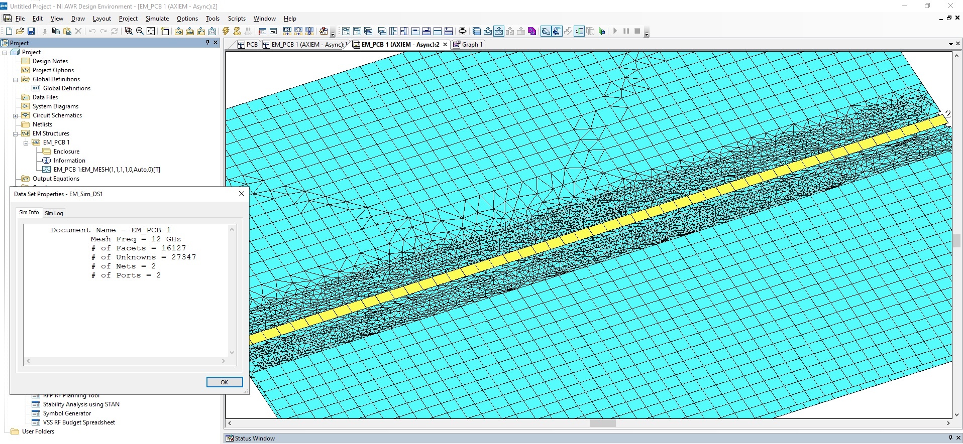
A finer mesh forms when your analysis frequency is higher. As a result, the number of unknowns also grow resulting in a very long simulation time. Don’t forget that a finer mesh also means a lot more memory. Be prepared!
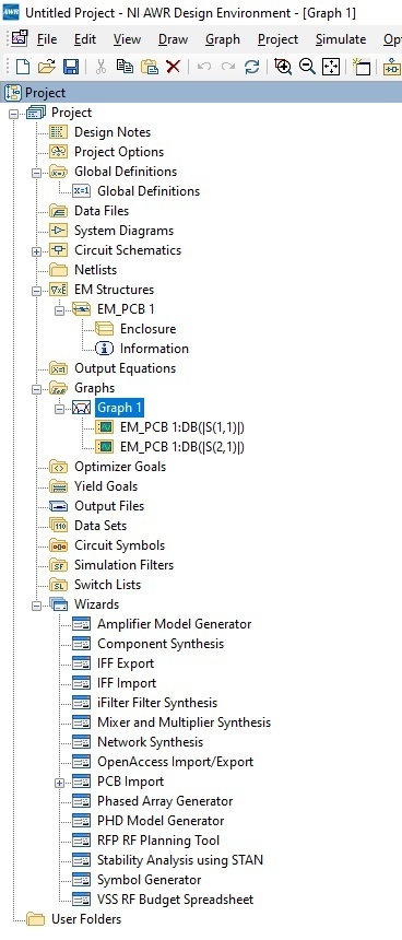
In order to start the simulation, right click on the Graphs > Simulate for Measurements.
The results
Simulation can be quite CPU intensive and you can see that in the screenshot below.
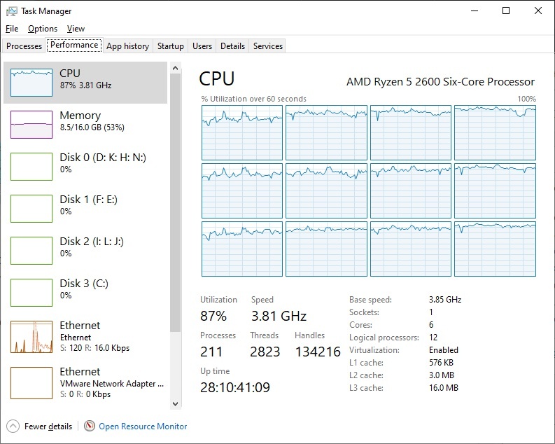
Observing the graphs closely, the CPU usage hardly crosses above 90%. This is an indication that our CPU is sufficiently fast. I ran the same simulation on an Intel i7 7700 and it instantly hit 100% on all the cores. Correspondingly, a full 100% usage is an indication of CPU bottleneck.
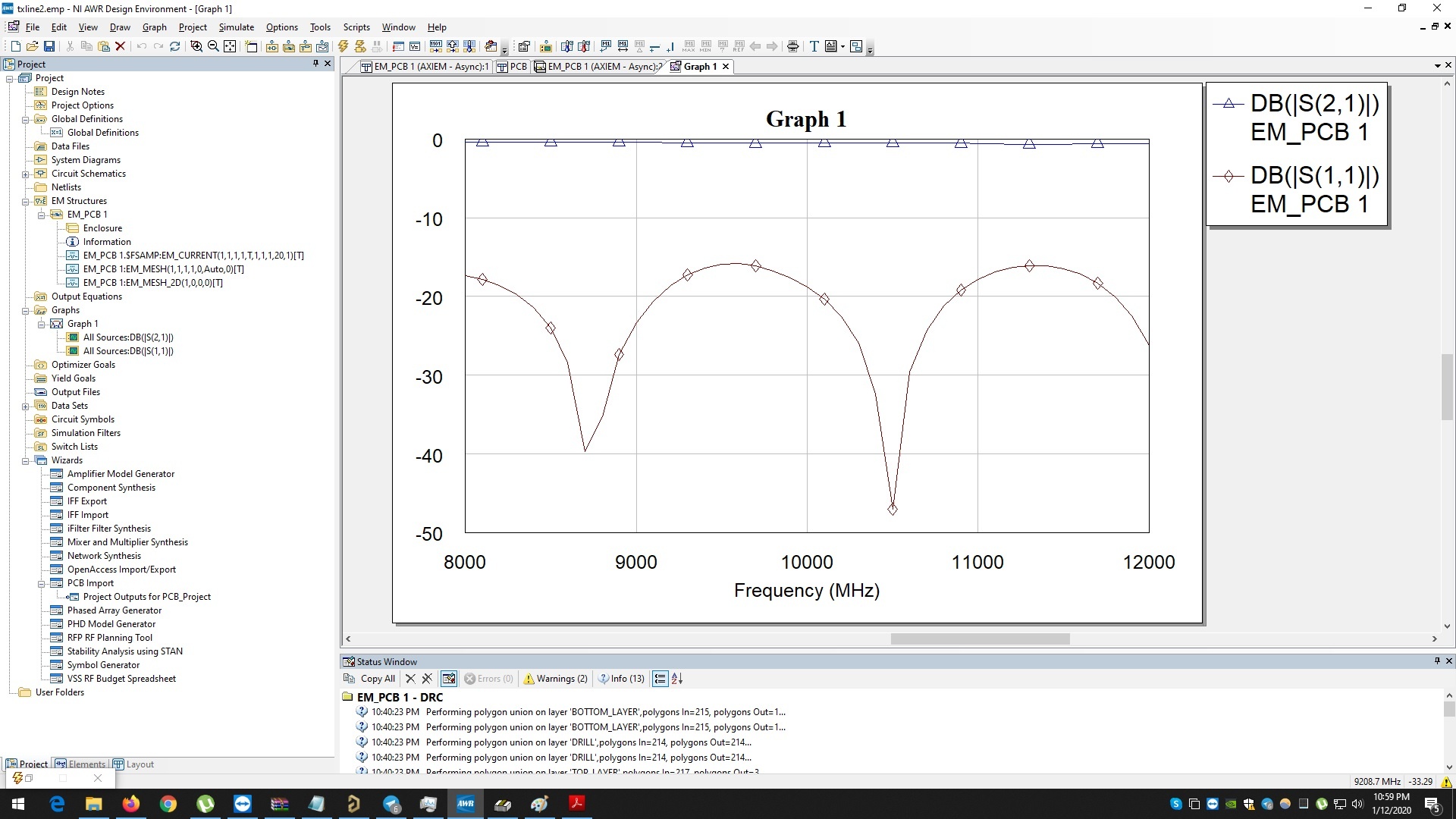
Here, we can look at the S parameter data coming out from the simulation. Apparently, the results are not that appealing. It could be improved further. While you try the EM simulation tutorial, I will get busy optimising my transmission line to target atleast -30dB return loss.
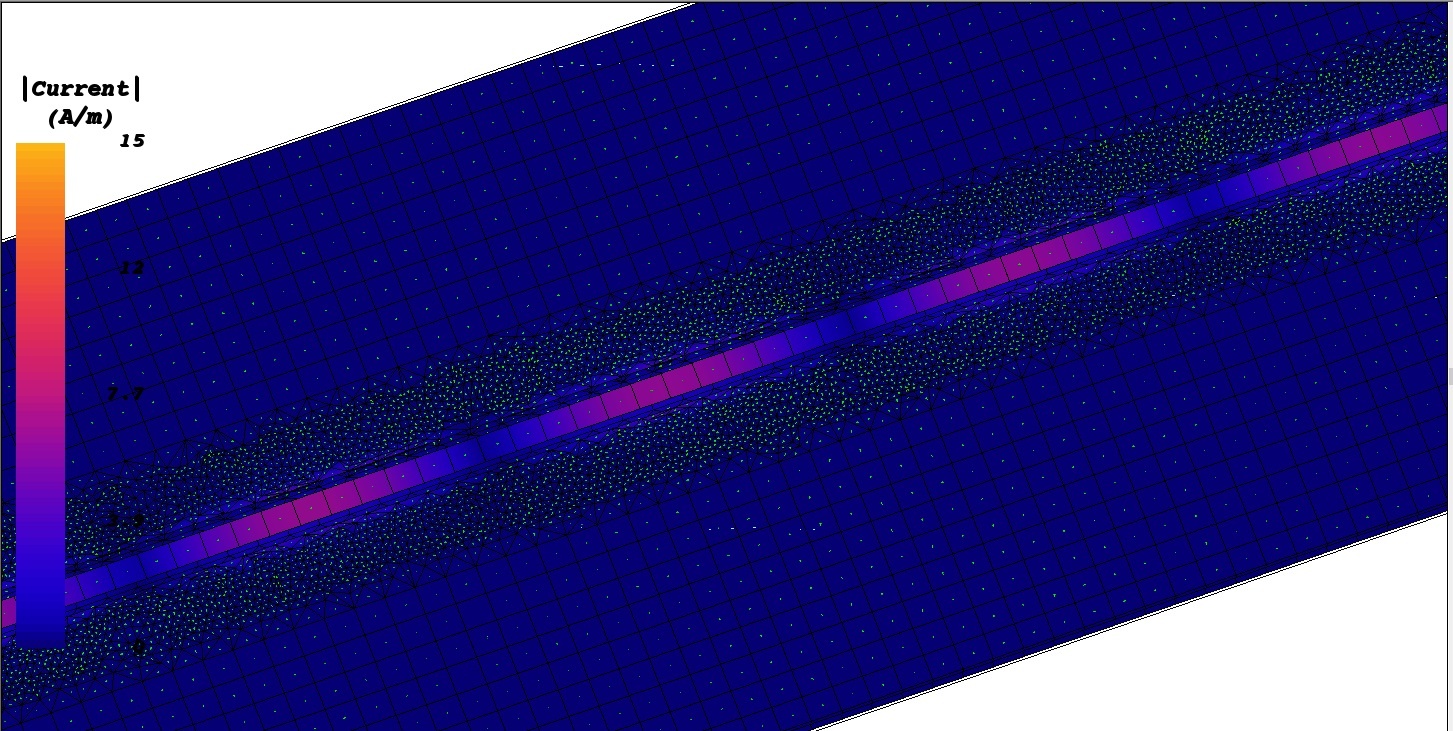
If you enable certain output parameters, you can also look at the cool EM fields.

If you’re just doing planar PCB stuff then it’s a lot easier (and faster) to use the Sonnet electromagnetics sim, imo. AWR is such a hassle to set everything up for a sim. I can do the same in a tenth of the time with Sonnet. Still, cool post.
Thanks for letting me know. I will have a look.