
A basic on screen display with Vivado HLS and Zynq SoC – Part 2
We created a very crude on screen display using HLS in the previous post. Now, it’s time to export it as a custom IP and integrate into the system. The process may seem to be a lot to take if you are doing it for the first time. Once, you are familiar with the workflow, you will be spinning out designs like no big deal. For someone who is totally new to Vivado and Vitis workflow, you should head on to one of my previous articles and try out a basic example.
Exporting the HLS IP Core
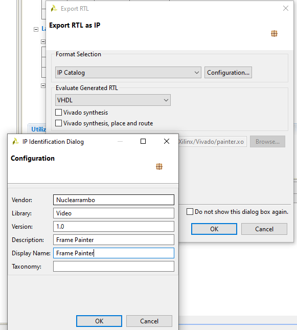
Doing this part is simple. I already tested the functionality of the code through C simulation and also RTL Co-Simulation. If you have correctly specified the FPGA device and the target frequency, everything should go smooth. Simply click on the Export RTL at the top and it will ask you somethings. Make sure you follow the screenshot below.
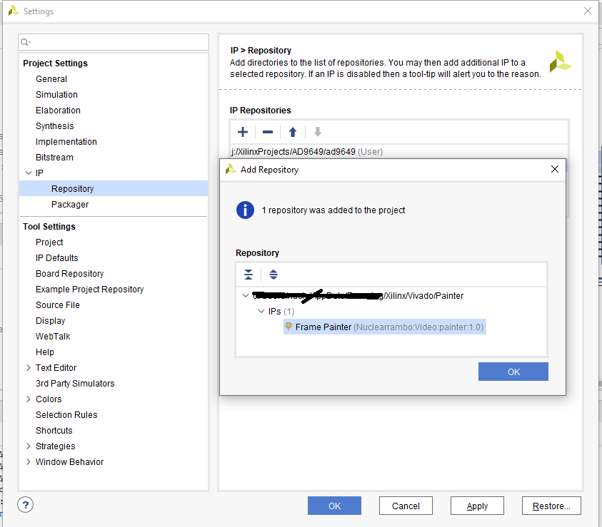
After the process is complete, open Vivado. There, you need to add the path to the IP core. Go to Settings > IP > Repositories and add the path to “Solution1”. This folder is found inside the HLS project folder. Vivado will now automatically identify the exported IP Core.
Setting up the system
I would like you to know at least the basics of setting up Zynq Processing System in Vivado and running some program on it. If you haven’t done anything like this before, I strongly suggest you head back to the very first tutorial I wrote earlier.
VDMA
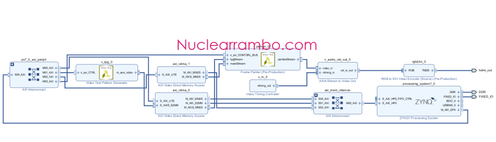
Before we proceed, let us try to understand the system plan here. There will be two VDMAs, one test pattern generator and our Painter HLS IP. The test pattern generator outputs test video over AXI4 Stream. Further, the streaming video is dumped into the DDR memory for buffering using VDMA. On the other hand, Zynq PS will write a 1280×720 RGB pixel mask onto the DDR memory section. A second VDMA configured in Read only mode picks up the data on this section and feeds it to our HLS IP Core.
DDR Access
The VDMA accesses the DDR through the HP0 port of the Zynq PS. On chip, hardwired DRAM controller handles all the interaction between DDR RAM. The MM2S (memory mapped to stream) and S2MM (stream to memory mapped) ports of the VDMA are all routed through the AXI4 Interconnect which also does the task of arbitration before finally connecting to the HP0 port.
On the other hand, the AXI4 Lite interfaces are routed through the second AXI4 Interconnect which is connected to the GP0 port of the Zynq PS. That way, a single AXI4 Lite Master on the Zynq PS can talk to several logic blocks through the AXI4 Interconnect.
Custom HLS IP Core
The output of the HLS Painter IP is also in AXI4 Stream video format. An AXI4 Stream to Video IP from Vivado IP Catalog converts the video into standard RGB video output. The Video output IP needs two inputs, one is the AXI4 Stream video and the second one being video timing signals. Correspondingly, the Xilinx video timing controller provides necessary timing and synchronization signals to the stream converter IP.
The Clock frequency and frame rate
The clock frequency can be set by double clicking the Zynq PS block and navigating to the Clock settings. Based on the video frame rate, the clock has been set to 111MHz. I came to this frequency value by a simple calculation.
\(F_{px} = MAX\_HEIGHT \times MAX_WIDTH \times Frame\Rate\)As decided earlier, the height and width are 1280 and 720 respectively. Additionally, the frame rate desired is 60 frames per second. The result comes to a number of 55.29MHz.
The Zybo board has an HDMI output port. To use that, Digilent provides a custom RGB to HDMI conversion IP core which you can download from here.
I am also attaching the project tcl file for anyone who wants to reproduce the project.
Configuring everything in Vitis
A lot of the IP cores used here require configuration over AXI4 Lite port. For example, the VDMA read write memory addresses need to be set. We also need to tell the VDMA when to start memory transactions. Additionally, all the HLS IP cores also require a start command to begin their work. Finally, we also need to set the mask in the memory. To do all this, we need to take some help from the Zynq PS.
Go to Vivado > File Menu > Export > Export Hardware > Include bit stream and finally export it all. You will end up with a .xsa file in the project folder.
Now you can fire up Vitis and start in a fresh workspace. Usually, I create a sdk folder inside the Vivado project and set up my Vitis workspace there. Fresh for every new project and it works well that way.
Create a new application project. While doing so, you need to add your own platform that you exported from Vivado. You can again refer to my previous Zynq post here to learn how to do that. Remember when you exported your HLS core? It also exported some basic C drivers to get you kick started immediately. Thats the beauty of automation and thats also how our future is going to be. The exported drivers can be found in the “drivers” folder situated in your project directory.
There are two options from here on. You either write everything from scratch or you use the source files I provide on Github. I will explain certain sections of the code but most of it is based on the vdma_api.c provided by Xilinx in xapp1218.
The C code
Defining the base addresses for the VDMA becomes our starting point because everything revolves around it.
|
1 2 3 4 5 6 7 |
#define VDMA0_BASE XPAR_PS7_DDR_0_S_AXI_BASEADDR + 0x1000000 #define VDMA1_BASE VDMA0_BASE+0x1000000 #define FRAME_HEIGHT 720 #define FRAME_WIDTH 1280 #define PIXEL_DEPTH 8 #define COLOUR_CHANNELS 3 #define FRAME_SIZE FRAME_HEIGHT * FRAME_WIDTH * COLOUR_CHANNELS |
We need to include our HLS IP driver header file called “xpainter.h”. Without this, we won’t be able to configure it unless you want to go completely raw and use the Xil_io API.
I then specify the instances for the IP cores I need to use. I also used the VDMA but that isn’t shown here. You can find it in the source code.
|
1 2 3 4 5 6 7 8 |
/* TPG Instance */ XV_tpg TPG; /* TPG Config */ XV_tpg_Config *tpgConfig; /* Painter */ XPainter Painter; |
Setting up the test pattern generator is a breeze while using the C API. The auto generated drivers for our IP core also make it absolutely easy to configure it. If you can do it for one, you can do for any other HLS based IP because the API structure is quite similar.
|
1 2 3 4 5 6 7 8 9 10 11 |
tpgConfig = XV_tpg_LookupConfig(XPAR_V_TPG_0_DEVICE_ID); XV_tpg_CfgInitialize(&TPG, tpgConfig, tpgConfig->BaseAddress); XV_tpg_Set_height(&TPG, FRAME_HEIGHT); XV_tpg_Set_width(&TPG, FRAME_WIDTH); XV_tpg_Set_bckgndId(&TPG, XTPG_BKGND_RAINBOW_COLOR); XV_tpg_EnableAutoRestart(&TPG); XV_tpg_Start(&TPG); XPainter_Initialize(&Painter, XPAR_XPAINTER_0_DEVICE_ID); XPainter_EnableAutoRestart(&Painter); XPainter_Start(&Painter); |
Doing the “EnableAutoRestart” is necessary otherwise, the IP core stops after one transaction.
Before we configure and start the VDMA, it’s necessary that we lay out the mask image in the memory. In the Part 1 of this article, I created a mask and saved it in BMP format. Open this image in hex editor such as the HxD viewer. Delete the first 54 bytes (0x36 in hex) and do this: File > Export > C. This will generate a C file containing your mask. It will be a large file considering the image size. Paste this C file in the src folder so that you can view it in Vitis.
Before we do anything with this file, let us let our C compiler know that the data we want to access is located in another file. We do this by using the extern keyword.
|
1 |
extern unsigned char rawData[2764800]; |
There are two ways for VDMA to see this data. One option is to provide the address to this array or copy this array to another memory location. I did the latter.
|
1 2 3 |
for(i = 0; i < InstancePtr.MaxNumFrames; i++){ memcpy((void*)(VDMA1_BASE+i*FRAME_SIZE), rawData, FRAME_SIZE); } |
Configure the VDMA
This part is relatively easy because the vdma_api.c from xapp1218 does most of the hard job for us. Although, I did a few changes in that file to configure the “read only” vdma. There are two things we need to take care of. When VDMA has no write channel, the “FrameSync” and “Genlock” mode need to be disabled. Secondly, you must not run any configuration pertaining to the write channel or else the code will fail. I have uploaded the modified vdma_api file to the github repo.
Does it work?
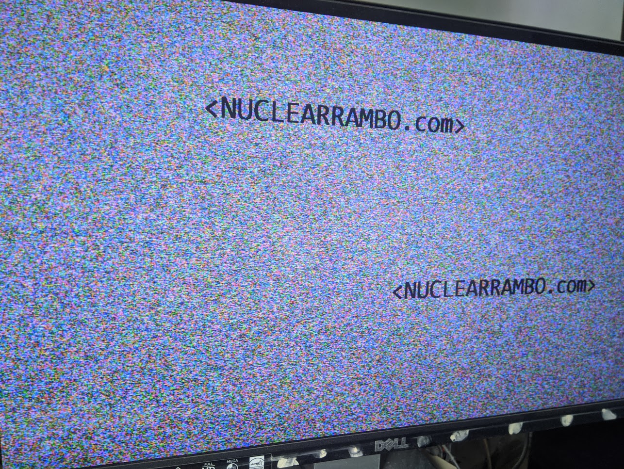
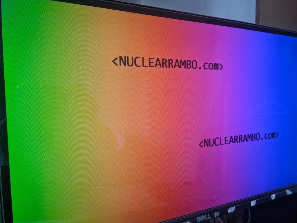
The mask contained text in two places and I expect the text to appear black.
In the second test, I generated random noise from the TPG and see how it performed.
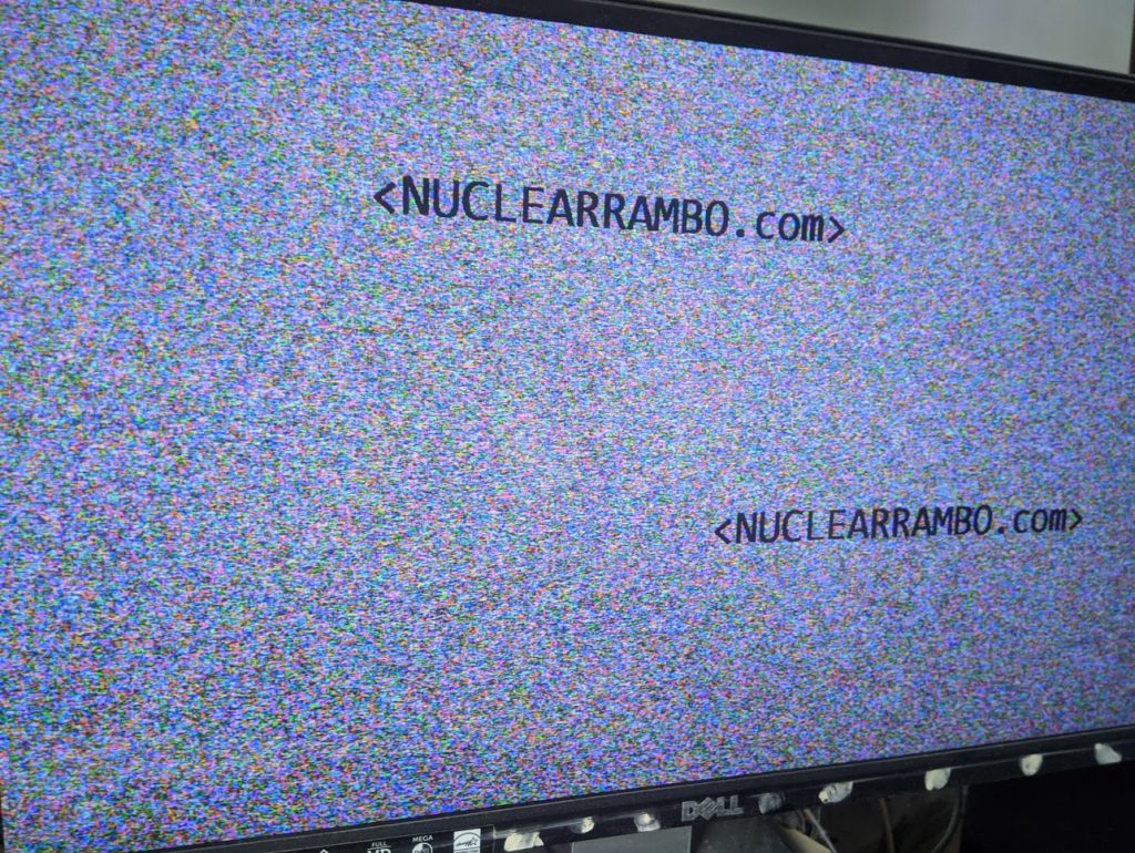
Everything seems to be working pretty fine. If you have any questions you can comment below.
Why is the frame rate multiplied by 2 in the calulation : Fpx = Max Height * Max Width * Frame Rate * 2 ?
In the calculation to find the Clock Frequency , Why is the product of Max Height, Max Width and Frame Rate multiplied by 2 ?
Thats a mistake, thanks for pointing it out.
Hey, do you have the full vivado project uploaded? I would like to see all of it and the block design in detail.
Unfortunately I do not have the project files anymore. If you do need help creating it, I will be happy to help.