
LM2731 boost converter in Altium Designer – From schematic to PCB
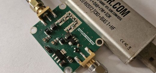
In this quick article, I show step by step process of drawing a boost converter schematic and finally ending up with a PCB layout. All of it done on Altium designer using Altium’s own Manufacturer Part search for component database. Although, I might use a few components from SamacSys free library. The circuit is based around LM2731 boost converter chip from Texas Instruments. I used this simple chip sometime ago for 5V to 12V conversion required to control a UHF amplifier. While some of you may say, why not just derive the 12V from the main DC supply? That would have been ideal but when dealing with high voltage DC, things get expensive fast. I felt this was the cheapest option for me. Anyway, my design choices are not the focus of this article. So, let’s get to the main business.
Selecting components and drawing schematic
The ideal option would be creating your own library components where every parameter is under your control. That way, we can standardize our library creation. Library creation can become a bit time consuming when it comes to maintaining every small parameter for documentation purpose. That’s all good when you are working in a professional setup. When it comes to doing circuits for hobby or quick prototyping, I don’t really care about all that stuff. All I want is a resistor with a specific value and a package. I may pay attention to exact part numbers if my design needs to work at several GHz.
Manufacturer Part search in Altium Designer is a very handy tool to search for parts quickly. Now, I have been using the Panasonic ERJ series resistors and I found that there are variations in footprint from part to part. For example, a 10K resistor may have a fixed set of parameters such as footprint, value, part number, temperature range and so on. Another value from the same series may have or not have certain parameters. Now, as a hobbyist I don’t really care about it. As a professional, this is bothersome.
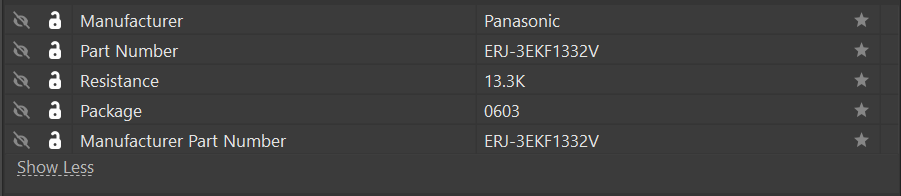
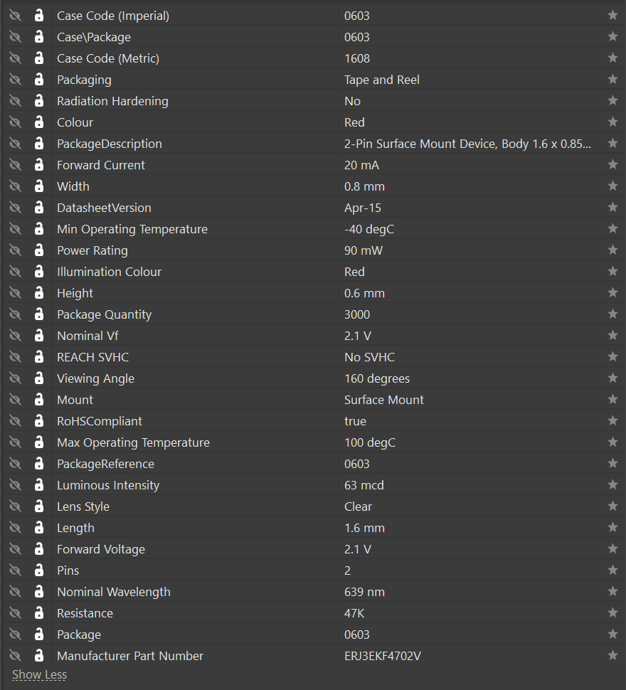
As you can see, the parameters for the 47K resistor don’t even match the resistor. Who specifies luminous intensity for a resistor? Clearly, whoever responsible for creating these part libraries isn’t doing their work correctly!
Nevertheless, I am bothered about the symbol and the footprint. Since, that’s meeting my requirement I am all good.
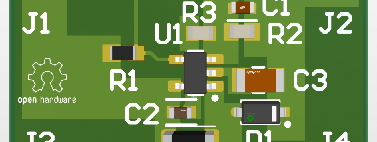
I carefully place all the symbols and create a small schematic quickly.
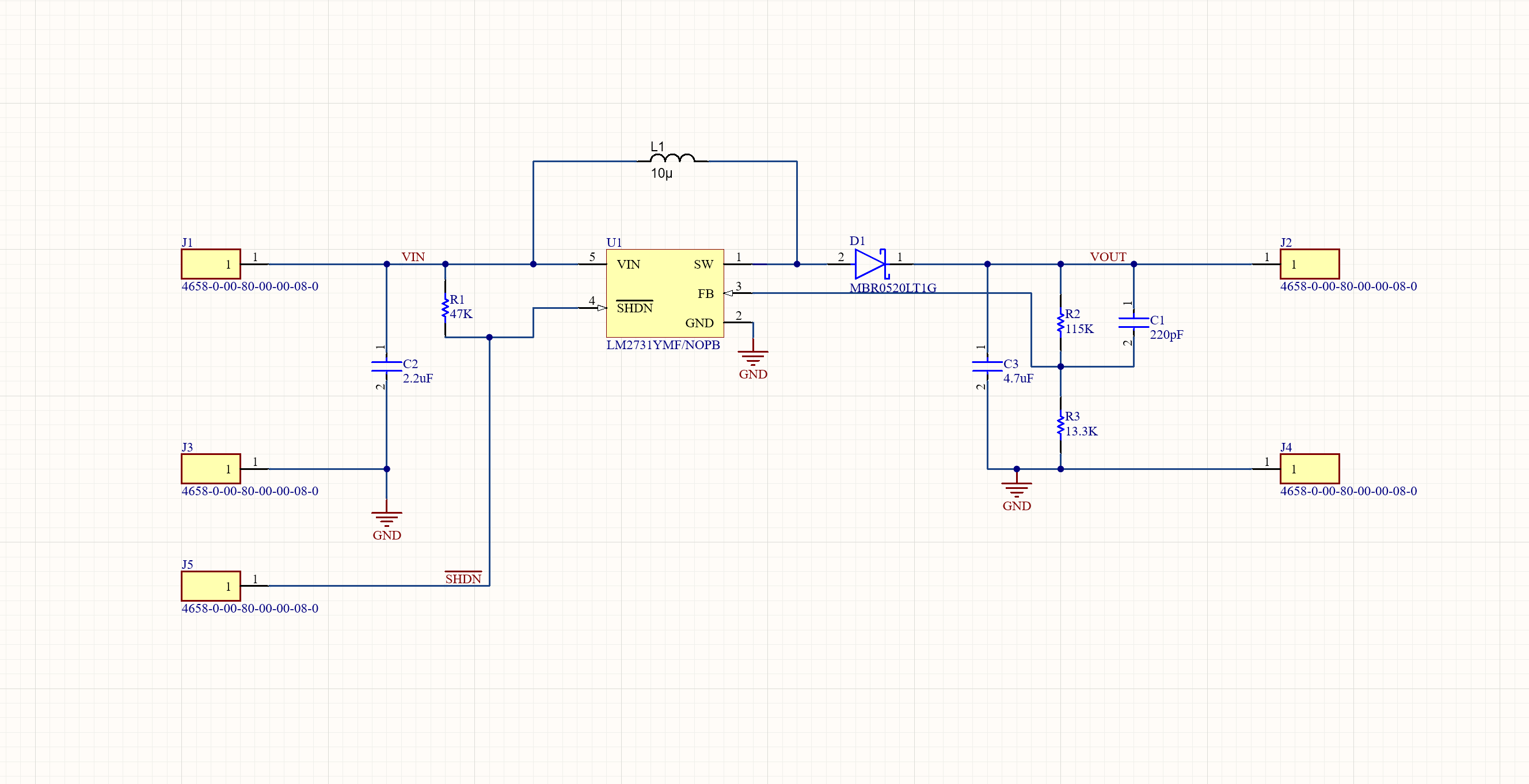
The input and outputs are turret terminals which I got from SamacSys library.
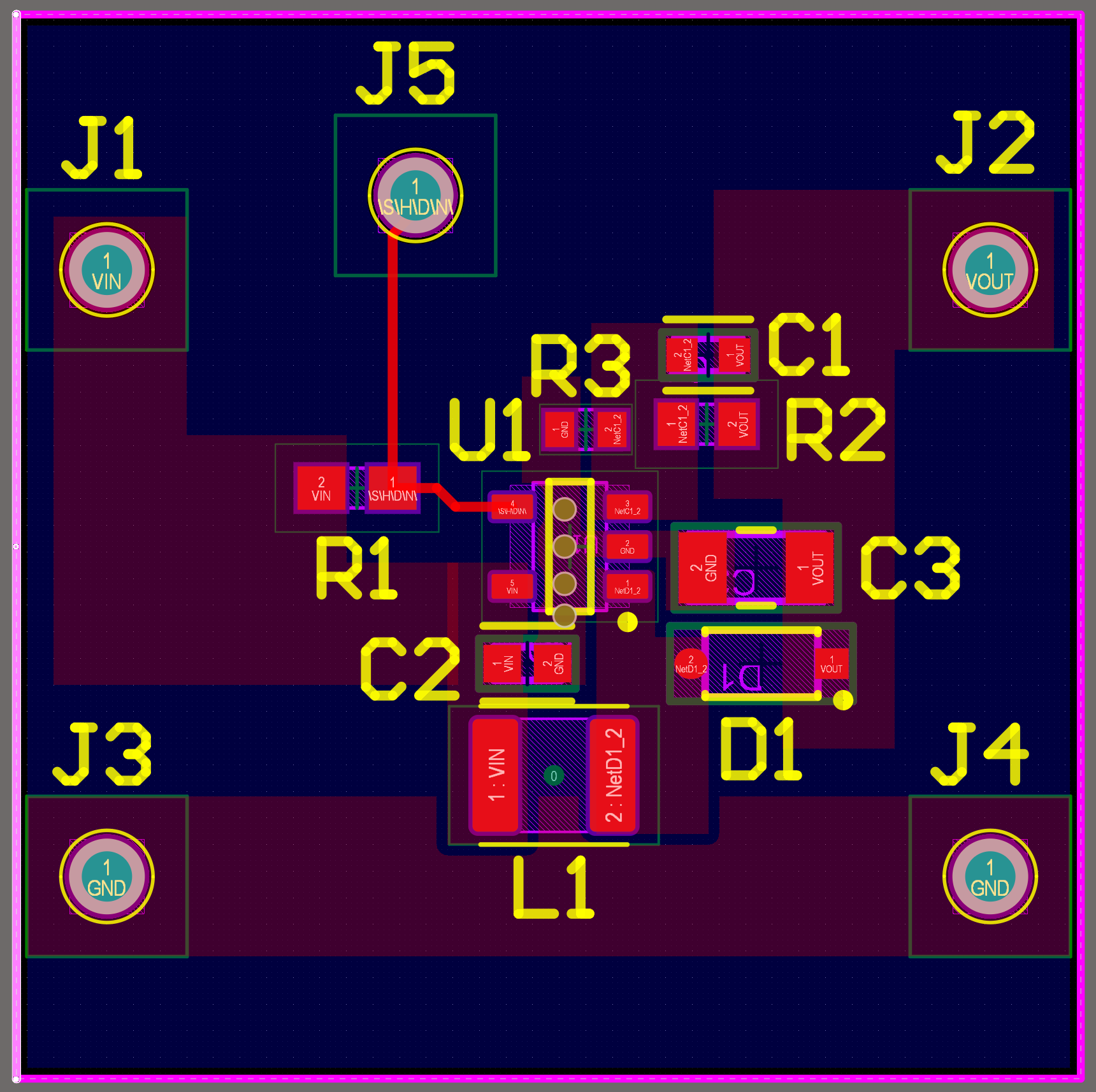
Layout
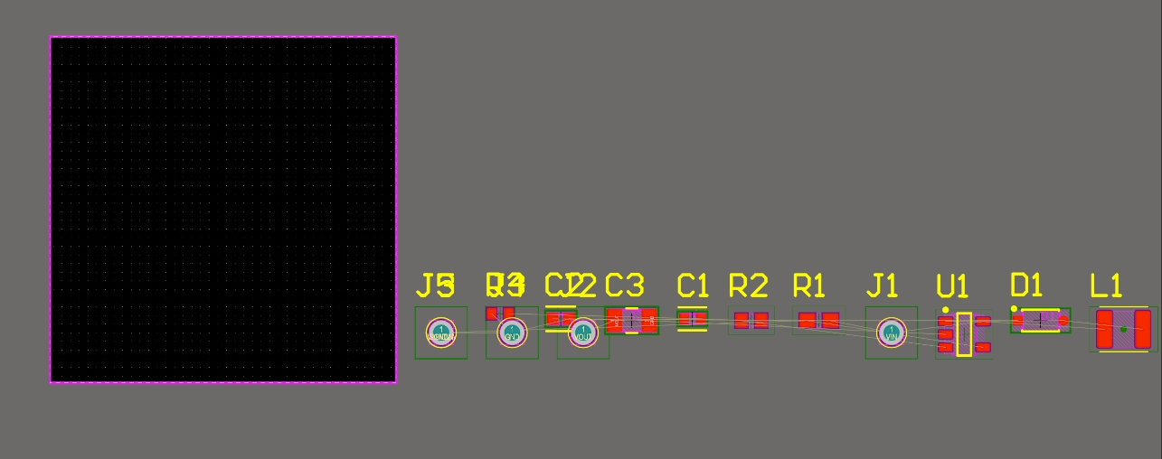
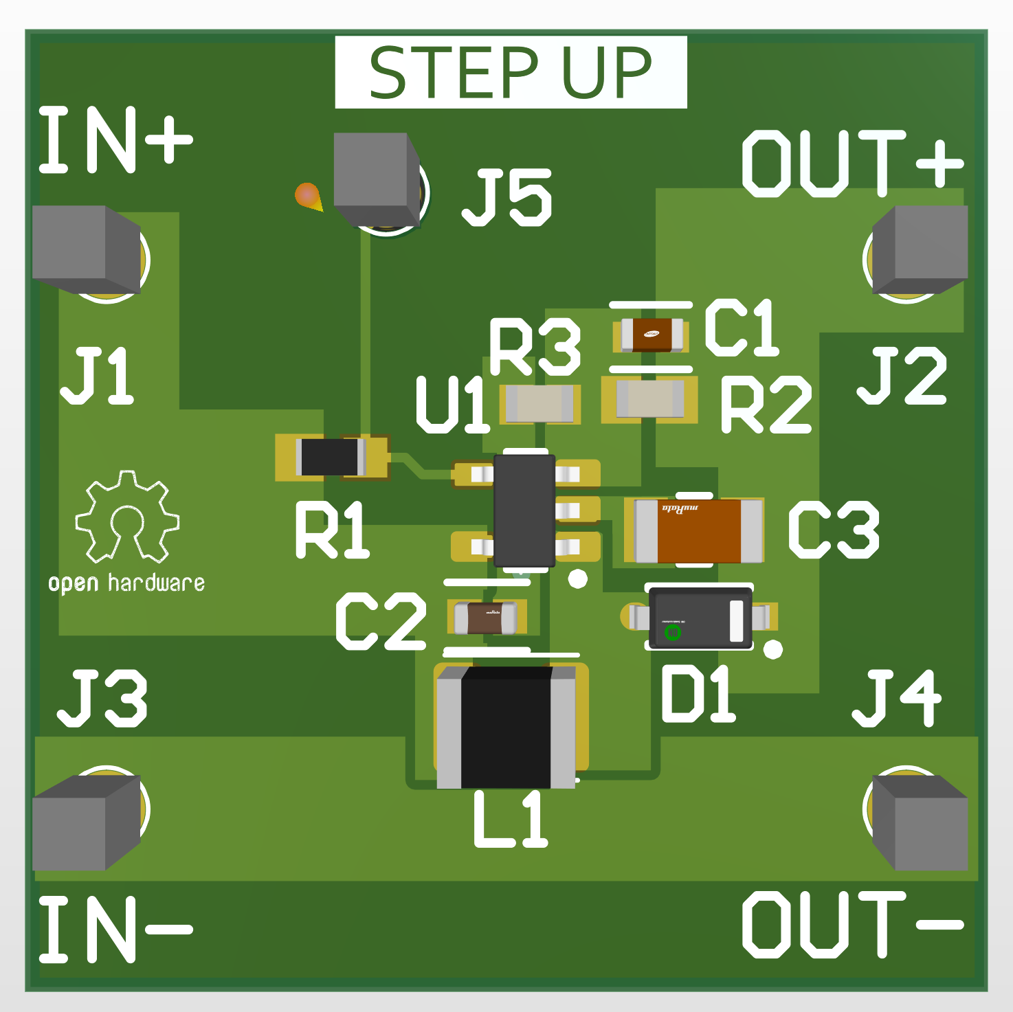
Considering the small number of components, I plan on laying everything in 1 sq. inch area.
First, I created a PCB document in the same project and saved it. Then, I imported all the components into the PCB. If you have your libraries set right, you should have no errors while executing the process.
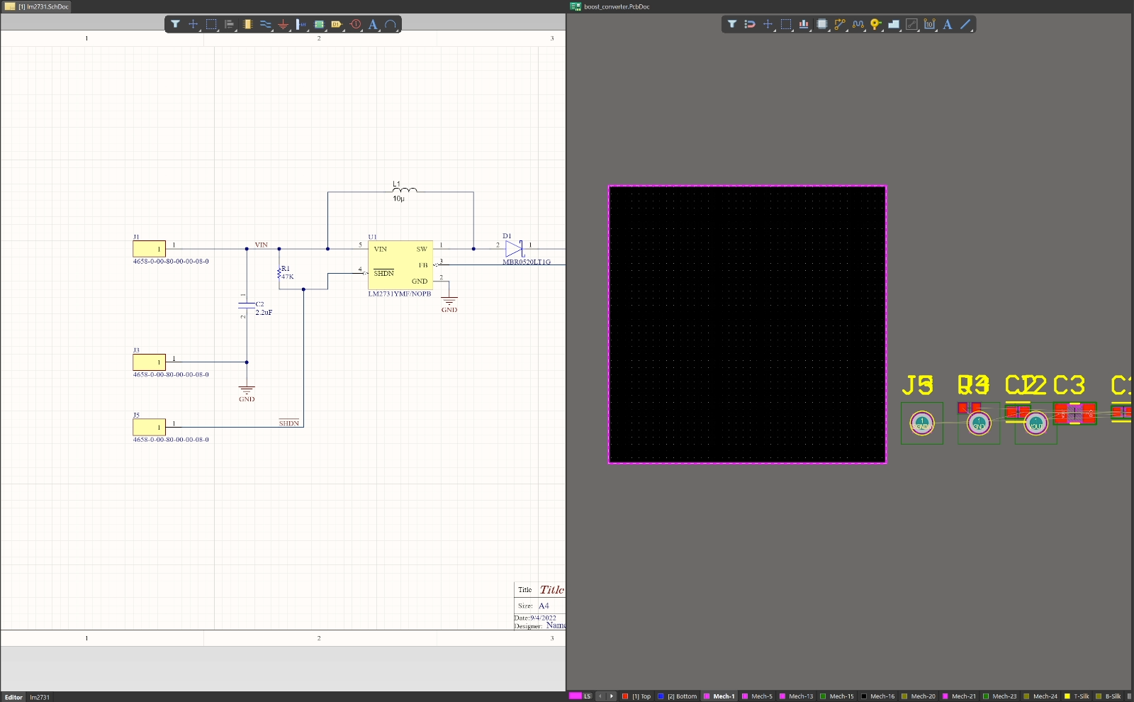
Splitting the screen vertically helps us to see both the documents simultaneously. Having a large 4K monitor makes a huge difference. Additionally, a second monitor makes life even easier. Enabling cross probe will let you select the respective component on the PCB while clicking on the schematic part. This is absolutely helpful when doing large schematics.
Let’s start placing components.
Mechanical components such as connectors need to be placed on the PCB first. Such components are usually the ones that connect directly to some other circuit or wiring assembly outside the PCB. Additionally, those may need to be placed in certain positions to meet mechanical constraints.
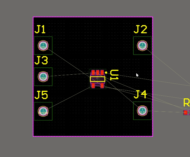
Second priority goes to the ICs. In our circuit, we only have one LM2731 boost converter chip, and we will place it in the center of the board. Rest of the components will come in next.
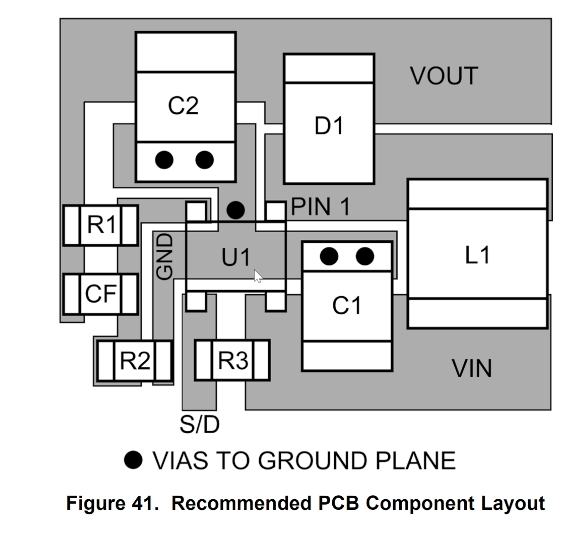
The input capacitor, inductor, diode and the output capacitor are the main passive components that need proper placement.
If we try to trace the current flow, this is how it would look.
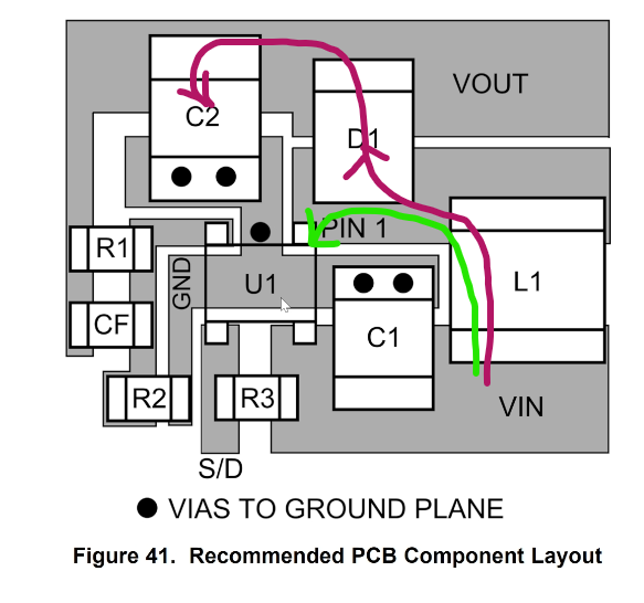
The Vin is the 5V input voltage from which current gets drawn (shown in pink), flows through the inductor, then through the diode and into the output capacitor. This flow happens when the internal MOSFET switch stays open. When the same switch closes, the current flows through the inductor, then through the internal MOSFET switch and finally into the ground. The diode ensures the charge stored in the capacitor does not discharge when the MOSFET shorts to ground.
Our layout must ensure that the current loop is physically small and stays as close as possible to the MOSFET switch which resides inside the chip.
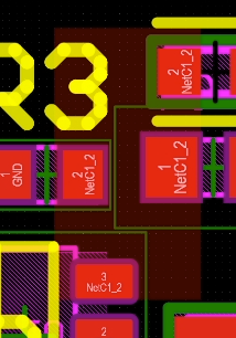
The resistors R1 and R2 in reference design are feedback resistors that help in regulating the output voltage. Changing these resistors will result in a different output voltage.
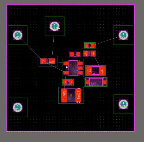
Now that we have initial placement ready, I will start routing.
Since, we are doing a boost regulator, we would like to keep trace inductance as low as possible. Laying polygons is one way to achieve that. The other option would be to layout fat traces. I am in favour of the first option because it looks nicer.
If you click on one of the nets while pressing Ctrl key, Altium will highlight all the nets with the same name thus, making it easier to know where to pour the polygon.
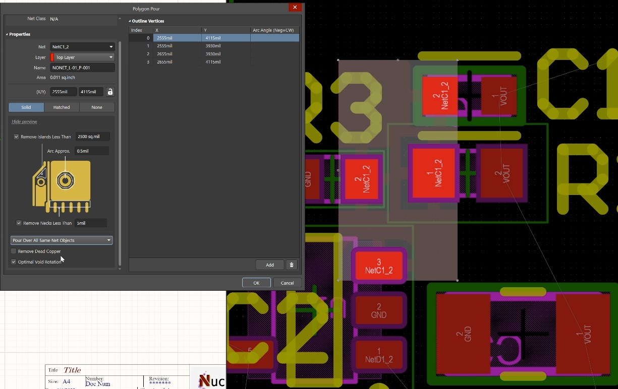
There appears to be one problem! We have thermal relief all over the connected pads. These thermal reliefs will add inductance. Let’s get rid of them by changing our rules.
Go to Design > Rules > Polygon Connect Rules > Select Direct connect.
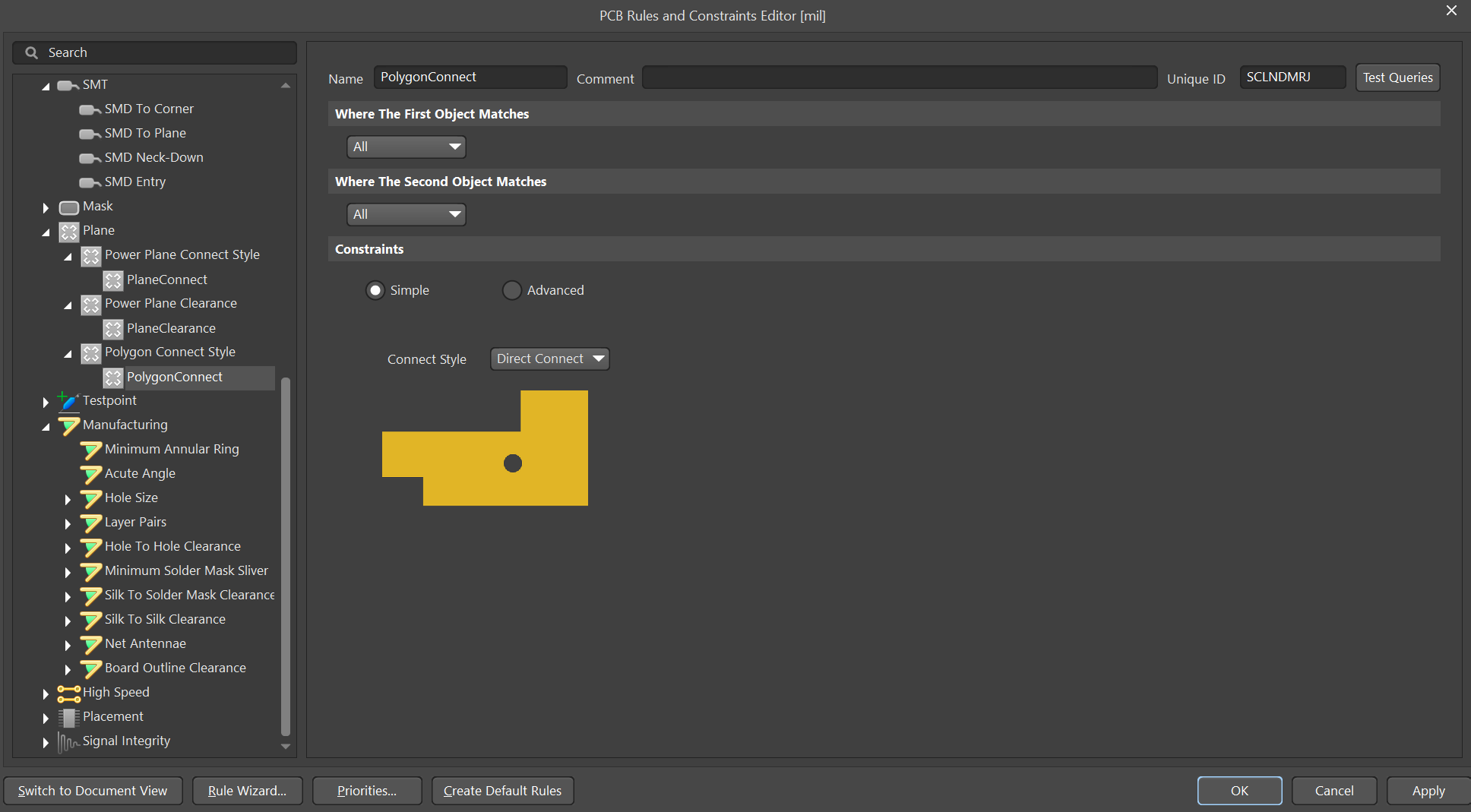
Now, repour the polygon by right clicking on the polygon > Polygon actions > Repour all.
Now, continue laying polygons on nets where high current would pass. Especially, around the input capacitor, diode, inductor and the output capacitor. You don’t necessarily need to add polygons around feedback resistor network.
Ideally, you wouldn’t want any ground polygon directly under the inductor. The right way to keep out polygon is to add a polygon cut-out.
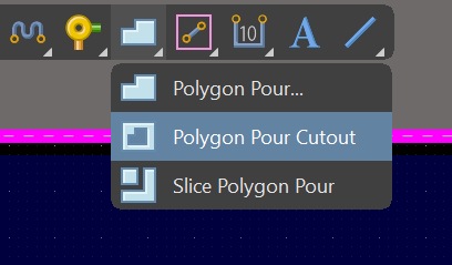
Place a small cut-out region under the inductor.
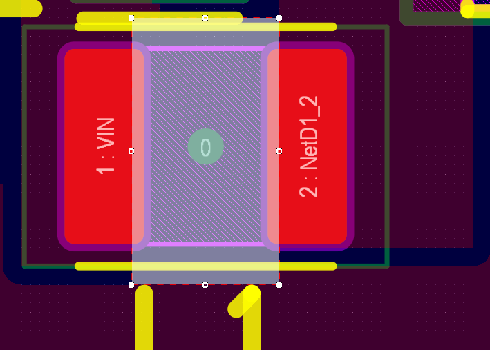
This small cut-out won’t allow any polygon pours underneath the inductor.
Additionally, you can add nice artwork on the top silkscreen. I will leave that to you.
Summary
While designing switching regulators, keeping a small loop size proves to be advantageous with respect to EMI. Usually, following the recommended designs yield good results but you can always follow an alternate route which you feel suitable. With this, we finish our small LM2731 boost converter PCB that converts 5V to 12V.
You can always access the design files from my Github repository.
If you are looking for a high-quality power supply, do check out this: Siglent Technologies SPD3303X-E

Voice of the people