
A short tutorial to simulate your Kicad PCBs in openEMS using Gerber2EMS
OpenEMS, an open-source tool for simulating electromagnetic structures, has been a valuable resource for the scientific community for some time. Its capabilities continue to expand, thanks to ongoing contributions that add new functionalities. While the openEMS package comprises various algorithms necessary for electromagnetic simulations, providing the required input can be tedious. Although programmatic interfaces via Matlab, Octave, and Python exist, they are not as user-friendly as commercial options like HFSS or CST Microwave Studio. Fortunately, this is gradually changing, making openEMS more accessible to a broader audience, including myself. One notable contribution is Gerber2EMS by AntMicro, which facilitates the use of Gerber files as input for openEMS to perform electromagnetic simulations..
Gerber2EMS is specifically made to work with KiCAD but with a little tweak here and there does allow one to use gerbers generated by any other PCB design tool. The installation process is quite simple if you are working on Windows. Things got messy when I tried to set it up on Linux. So, for the sake of this tutorial, I will be using Windows 11 and Python 3.11.
Installation
Before starting, install the latest version of KiCAD on your PC. Gerber2EMS relies on specific names used by KiCAD to identify various PCB layers. As a result, it won’t directly recognize Gerbers generated by other tools, such as Altium Designer. However, with a few modifications to the Gerber importer script, you can use Gerber2EMS with Altium-generated Gerber files.
Proceeding with our first step, ensure you have Python 3.10 or Python 3.11 installed on your computer. Download the openEMS package from the link and extract it to your drive. You don’t need to build the sources if you are using Windows 11. Follow the instructions below to install the Python packages.
|
1 2 3 |
cd C:\opt\openEMS\python pip install CSXCAD-0.6.2-cp310-cp310-win_amd64.whl pip install openEMS-0.0.33-cp310-cp310-win_amd64.whl |
Ensure you set the environment variable pointing to the openEMS folder below.
|
1 |
setx OPENEMS_INSTALL_PATH C:\opt\openEMS |
Your path may differ from the one given above. Therefore, ensure you enter the right path in your environment variable. Restart the terminal for the variable to come into effect.
Download Gerber2ems package from this link. For git users, simply run this command:
|
1 |
git clone https://github.com/antmicro/gerber2ems.git |
Go to the gerber2ems directory and run
|
1 |
pip install . |
This installs all the binaries for gerber2ems that can be called through Windows terminal.
Next, you need to install two more tools, gerbv and Paraview.
Gerbv comes in a zip package which needs to be extracted somewhere. Upon extracting, add the gerbv directory to your PATH environment variable. This is a very important step and should not be missed. I tried running gerber2ems without adding gerbv to PATH variable. I struggled for some time before realising the problem. After adding gerbv to the PATH environment variable, everything worked fine.
To test your installations, run the following commands in your command terminal.
|
1 2 3 |
gerber2ems gerbv |
Running examples
Antmicro provides four examples to try out and those can be found in the “examples” directory. Open a command terminal in one of the examples. I chose the example named “real” and opened a terminal inside the directory and run this
|
1 |
gerber2ems -a --export-field |
A correct installation should allow this command to run through and produce simulation results. The results end up in “ems” directory.
Based on the examples, I created my own PCB project for simulation. Read further to understand the process.
Co-planar waveguide simulation in gerber2ems
gerber2ems looks for three inputs necessary to carry out a simulation using openEMS.
- Gerber files inside “fab” directory
- PCB stackup file inside the “fab” directory.
- Simulation file in the project directory.
The PCB stackup
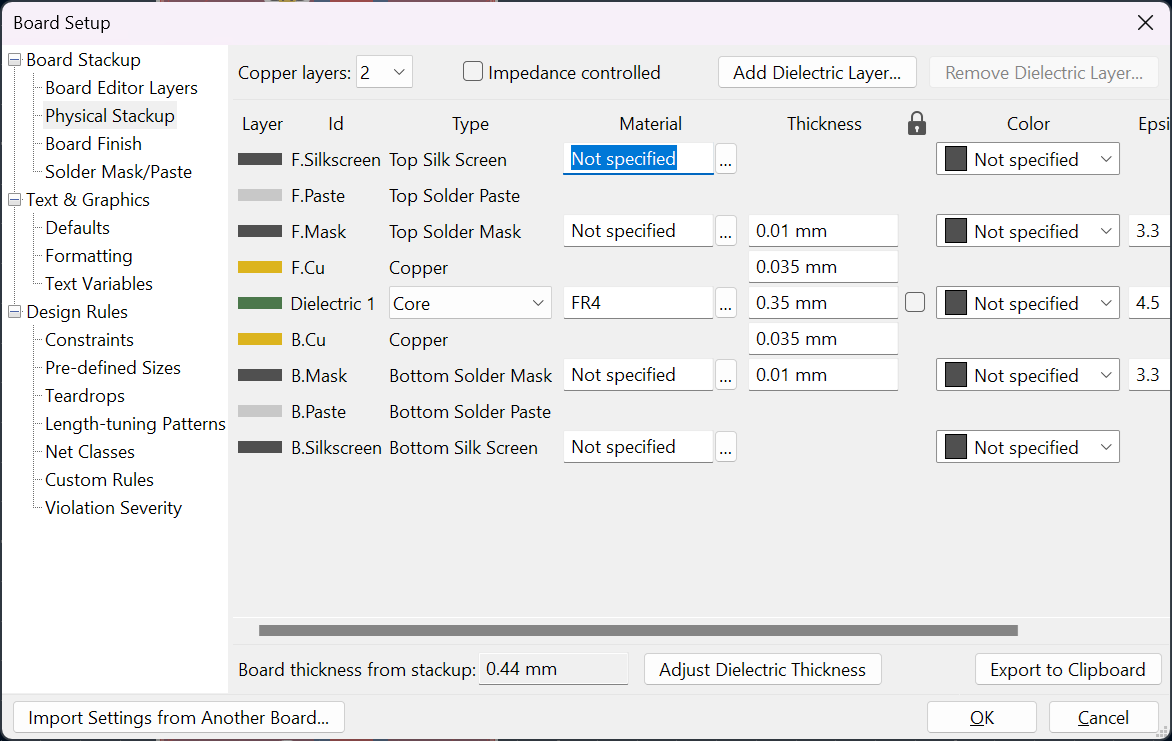
I took the “real” example as my basis to the simulation. My PCB stackup has a 0.35 mm FR4 dielectric. Correspondingly, I also changed the stackup.json file with the new values.
|
1 2 3 4 5 6 7 8 9 10 11 12 13 14 15 16 17 18 19 20 21 22 23 24 25 26 27 28 29 30 31 32 |
{ "layers": [ { "name": "F.Cu", "type": "copper", "color": null, "thickness": 0.035, "material": null, "epsilon": null, "lossTangent": null }, { "name": "dielectric 1", "type": "core", "color": null, "thickness": 0.35, "material": "FR4", "epsilon": 4.5, "lossTangent": 0.02 }, { "name": "B.Cu", "type": "copper", "color": null, "thickness": 0.035, "material": null, "epsilon": null, "lossTangent": null } ], "format_version": "1.0" } |
Add ports
On the PCB, add two ports on the F.Fab layer. I copied these ports from one of the example designs.
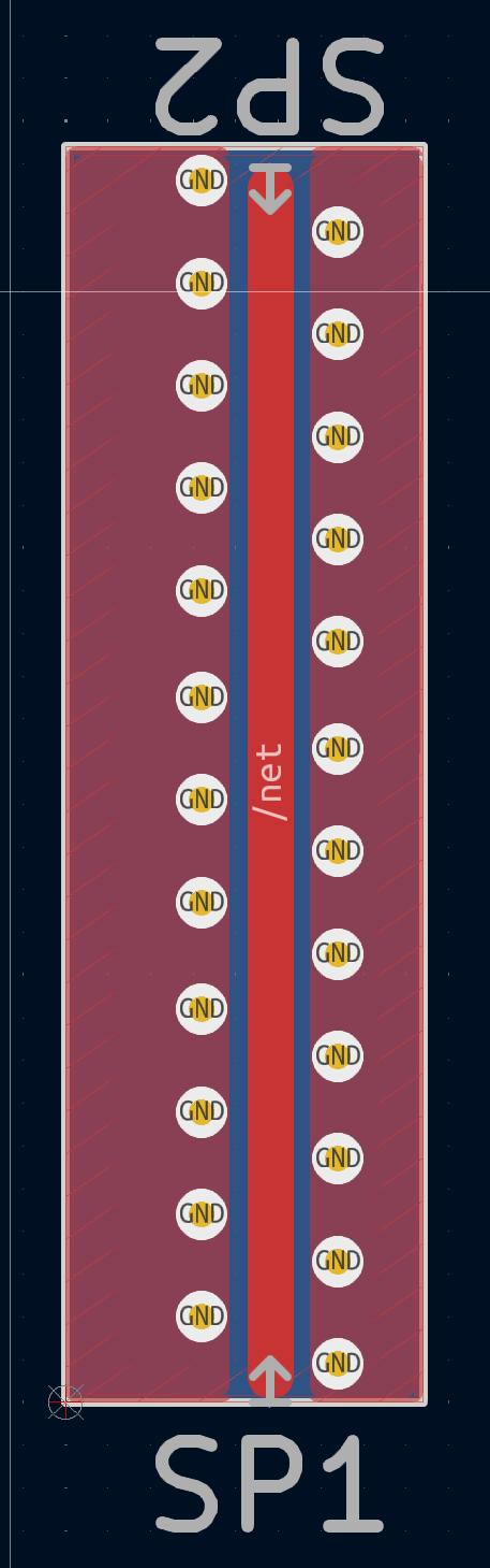
Make sure to add an outline to your PCB on the Edge_Cuts layer. gerber2ems uses the Edge_Cuts to identify the PCB shape and compute the port positions accordingly.
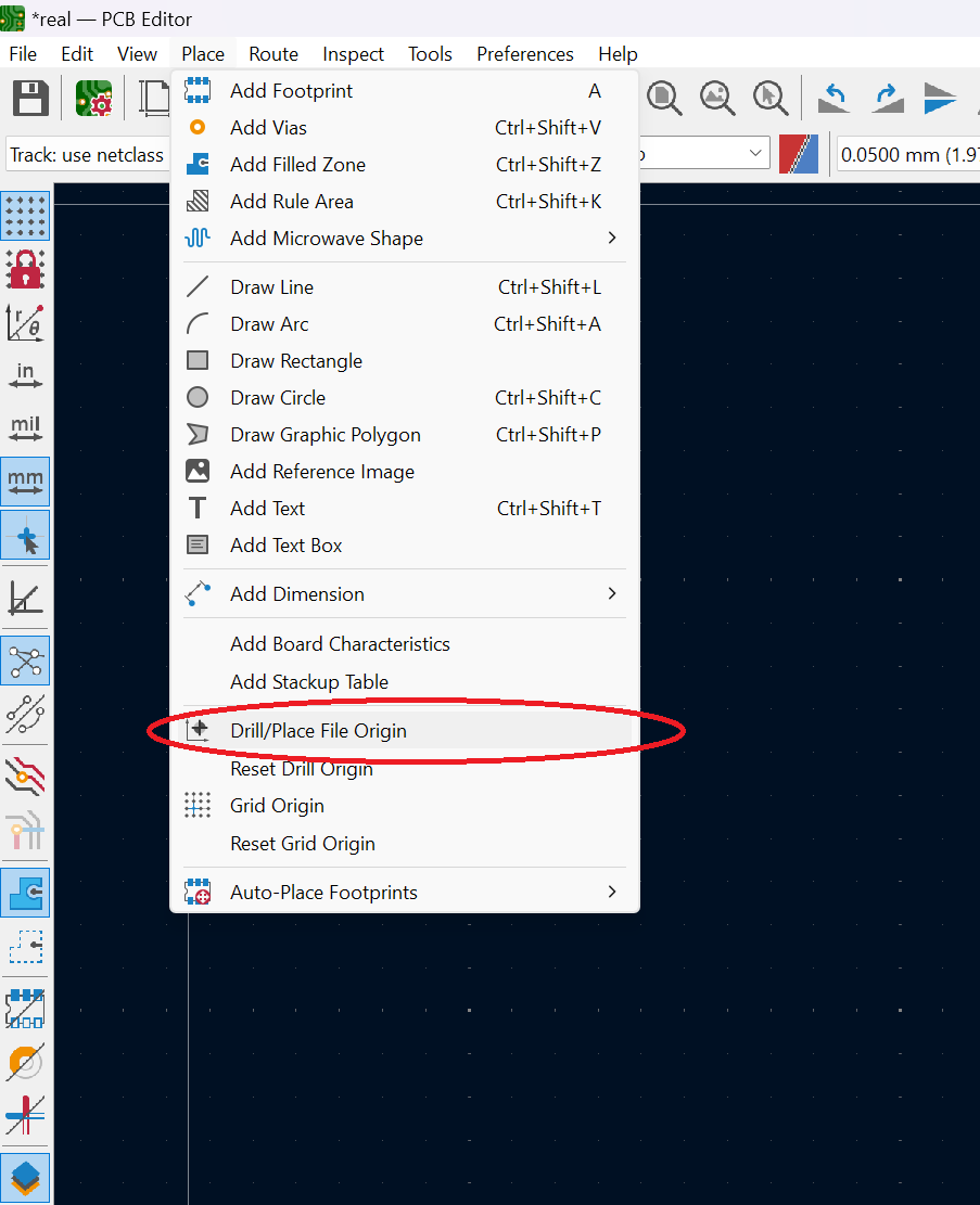
Speaking of the port positions, add the drill origin to the left bottom of the PCB outline.
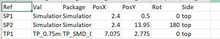
In the “fab” folder, there’s a file called “xxx-top-pos.csv” where xxx is your project name. This file contains the port positions calculated with respect to the drill origin. I don’t know a simpler way so I manually calculated those positions by subtracting drill origin coordinates with port coordinates.
For example, the drill origin is at (144, 90) and the SP1 port at (150, 95). The position for SP1 to enter into the CSV file would be (150 – 144) = 6 and (95- 90) = 5. Therefore, the SP1 position = (6, 5). Similarly, calculate for rest of the ports in your design. In this example, we only got 2 ports. Had it been a differential line or a 3 port network, we would have more than 2 ports.
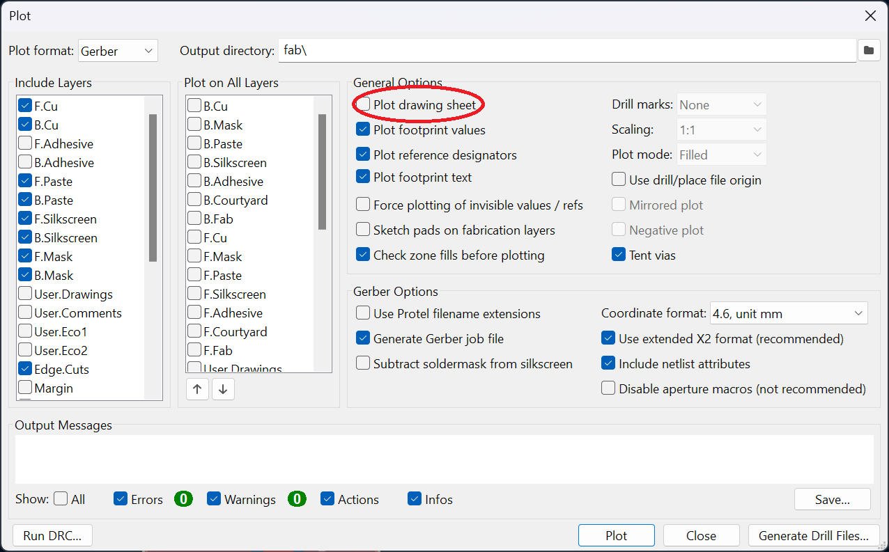
Finally, generate the gerber files and ensure you disable this option. In another design, I had this option enabled that confused the gerber2ems and repeatedly threw errors at me.
Simply adding ports to the design isn’t enough. These ports should also be added into the simulation.json file in the project root directory. It’s better to take reference of the example simulation file to start with.
You must set the start and stop frequencies for the simulation. Furthremore, select an appropriately sized meshing. To know more about the simulation parameters, refer to the official gerber2ems github link.
More about simulation settings
Going by the github link, the simulation.json file has three major sections; Miscelleneous, Mesh and Ports. The details for each section are provided on the github page.
Since, I copied the simulation file from the “example”, I only made minor changes to the parameters to suit my needs.
|
1 2 3 4 5 6 7 8 9 10 11 12 13 14 15 16 17 18 19 20 21 22 23 24 25 26 27 28 29 30 31 32 33 34 35 36 37 38 39 40 41 42 43 44 45 46 47 48 49 |
{ "format_version": "1.1", "frequency": { "start": 1e9, "stop": 4e9 }, "max_steps": 8e4, "via": { "filling_epsilon": 1, "plating_thickness": 50 }, "mesh": { "xy": 50, "inter_layers": 6, "margin": { "xy": 200, "z": 200 } }, "margin": { "xy": 1000, "z": 1000 }, "ports": [ { "width": 600, "length": 500, "impedance": 50, "layer": 0, "plane": 1, "excite": true }, { "width": 600, "length": 500, "impedance": 50, "layer": 0, "plane": 1, "excite": true } ], "traces": [ { "start": 0, "stop": 1, "name": "A" } ] } |
To summarise the setup, I created a CPWG, added two ports, modified the PCB stackup, modified the stackup.json to match the PCB stackup, generated the gerbers and finally edited the position file. Now, let’s run the simulation.
Running the openEMS simulation on your Kicad PCB
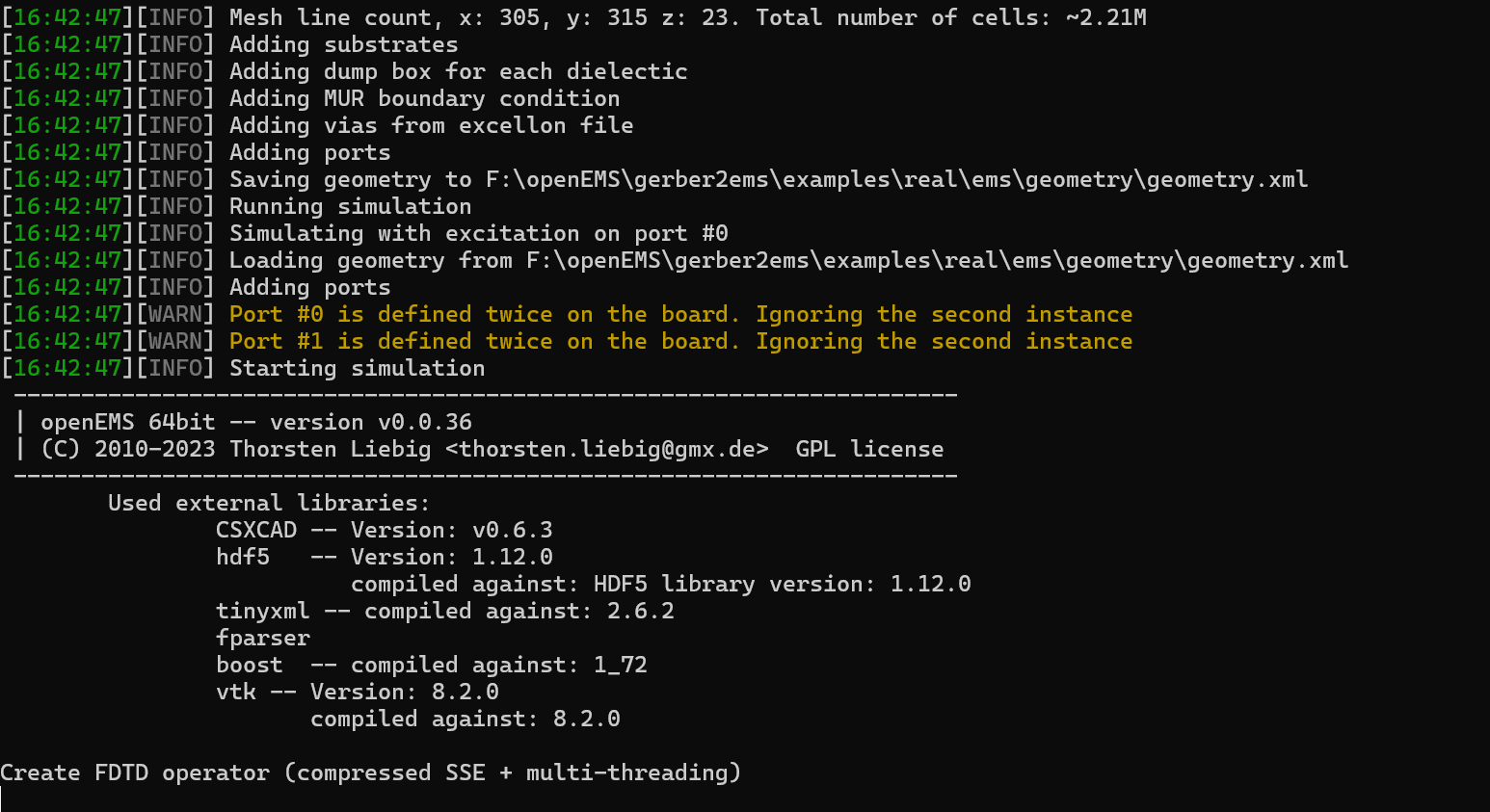
A correct setup results in error-free simulation. It’s imperative that you calculate the port positions correctly. Incorrect positions, mismatch between the CSV file and the PCB, results in inaccurate simulation.
Run the following command in your project root and wait for the results:
|
1 |
gerber -a --export-field |
Depending on your PC configuration, the simulation time could take time.
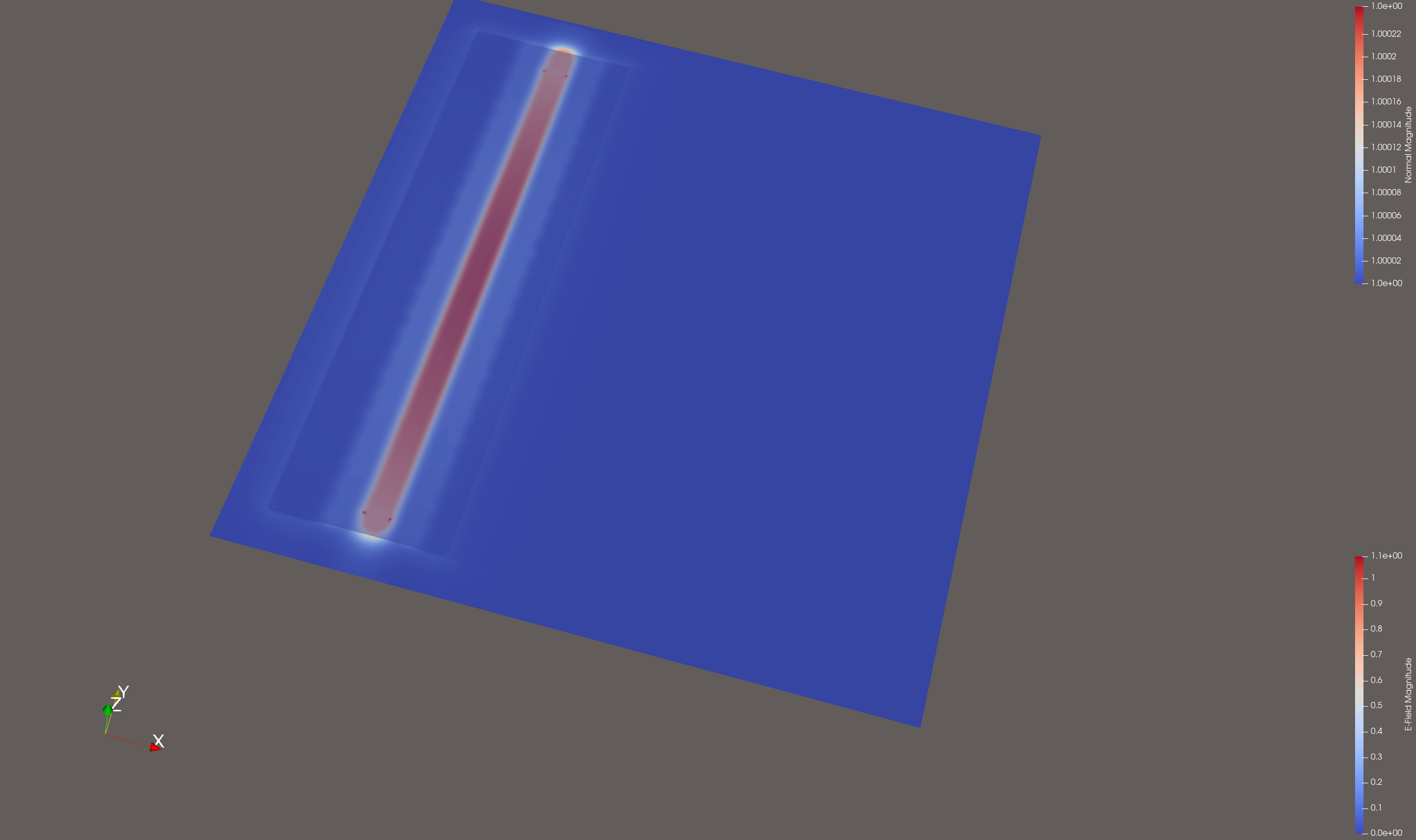
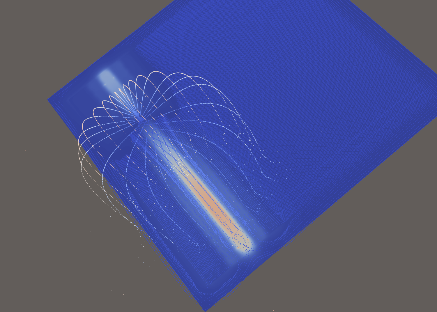
The results
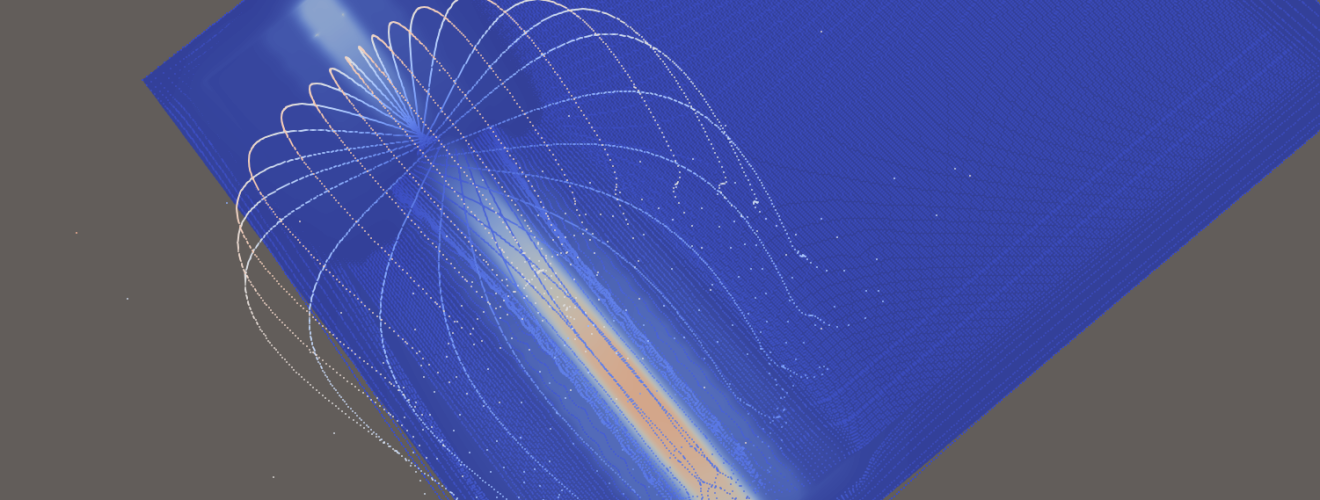
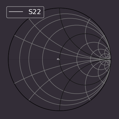
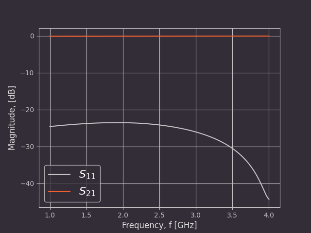
After a while, the simulation completes and dumps the data into the “ems/simulation/” directory. Now, we can either view these results using Paraview or simply observe the Smith chart produced by gerber2ems.
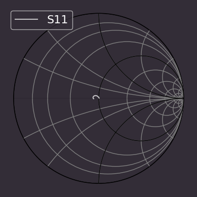
Wonderful! Gerber2EMS captured the simulation results from openEMS and computed the S-parameters eventually saving it automatically into an image. Upon closely observing, the smith chart reveals a not-too-bad CPWG. Additionally, gerber2ems also generated plots for delay, S22, S21, etc.
Let me know what you think in the comments below. I will be glad to answer any questions you may have regarding this article.
Thank you for the tutorial! This is very useful for people using Windows 11, Python and KiCad combination!
I was getting error of gbr files not being converted to png files and though maybe there was a problem with the gerbv installation. But then I saw that your gerber2ems folder was in the openEMS folder and moving mine there that solved the problem..
I’m glad it worked out for you.
First of all I want to thank you for the guide! One thing I however have been struggling with is how to simulate a PCB design with lumped elements, e.g. a PCB including resistors.
Gerber2ems may not support that directly. You may need to dig into the script and perhaps make changes to script taking reference from official openems examples.
Thanks for the tutorial! Had gerber2ems examples working, but I was struggling to get it working on my design, and this tutorial certainly helped.
I’m glad you found this post useful. Thanks for reading.
Hi,
I was able to follow your tutorial successfully using the provided example files—thanks a lot for that!
I’m currently working on running simulations with my own PCB designs created in KiCad 9, but I’m running into some issues generating the correct files for gerber2ems.
Would it be possible for you to share a minimal KiCad 9 project as an example? Even a simple 4-layer board would be extremely helpful in understanding how to properly set up the layer stack, file structure, and naming conventions.
I’m trying to simulate an antenna, but the Smith chart and S11 results are currently all over the place. Also, do you happen to know if there’s a way to perform far-field simulations with this toolchain?
Thanks again for your great work and any help you can offer!