
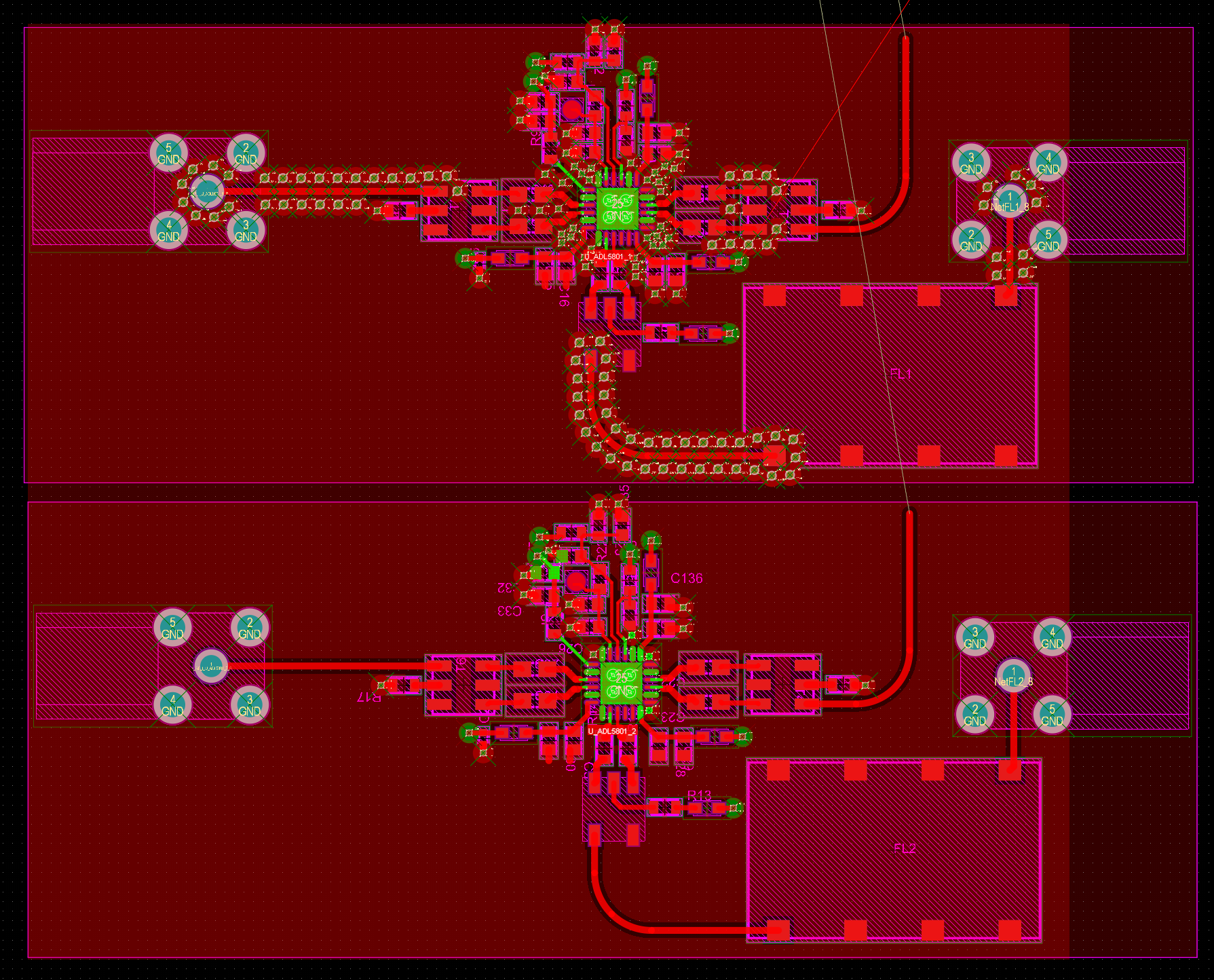
PCB layout of the ADL5801 RF mixer
The ADL5801 is a double-balanced active mixer with LO buffer. There is a provision of an RF detector inside the chip which can be used to bias and tune the output IP3 performance of the mixer. Additionally, this mixer gives an excellent linearity performance allowing it to be used for communication applications. It offers this performance due to its ability to auto-bias itself in the presence of large in-band blocking signals. When large blocking signals are present, the auto-bias causes an increase in overall noise figure of the mixer. In the absence of such large signals, the auto-bias tunes itself down, lowering the noise figure and reducing power consumption.
In this article, I show the process of designing a PCB for ADL5801. The mixer is part of a multi-channel RF front-end. Here, I explain the schematic then place the components and finally, route the mixer section. This circuit being part of a larger, multi-channel design, has 3 more identical mixer circuits. Altium Designer allows us to layout one circuit and copy the placement and routing to the rest of the identical circuits.
The schematic
I haven’t changed the schematic much from what Analog devices give as part of their reference design.
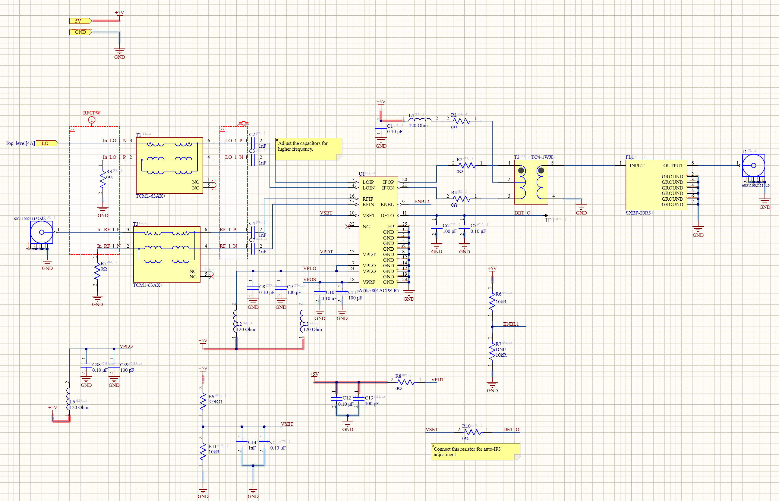
For the purpose of the target application, the LO comes from an RF power splitter sitting outside of this schematic view. It’s visible as a port on this schematic.
The baluns ensure the unbalanced RF and LO signals convert into balanced signals before being fed to the ADL5801 mixer. The 1nF capacitors on the differential LO and RF lines ensure AC coupling since the baluns are non-isolated. We don’t want any DC offsets present on these lines since that can cause a shift in mixer performance.
Similarly, on the output end, the IF port has a 200 Ohms impedance. A 4:1 balun helps us to interface the mixer to standard 50 Ohms circuits lying ahead. In this case, a bandpass filter.
Furthermore, I provide an option of setting the ENBL pin to either logic high or low. By default, this pin would be set high because that’s what gives the best performance according to the datasheet. Additionally, the detector output can be connected or disconnected from the VSET pin by either placing or removing the 0 Ohm resistor.
Placement
The placement of this mixer is quite straightforward without too much of a hassle.
I start by placing the components on the RF and the LO path.
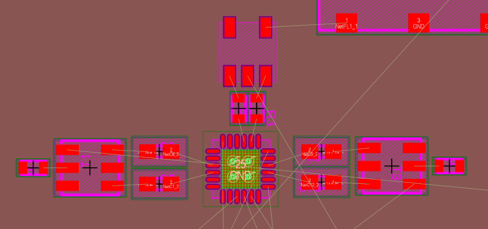
My application requires this circuit to work up to 4GHz at least. The DC blocking capacitors are placed as close to the chip as possible followed by the baluns.
Once the most important RF path components are set, I can proceed to place the rest of the passive components. These passive components are mostly responsible for decoupling noise on the power lines, enabling or disabling the chip, biasing connections and so on.
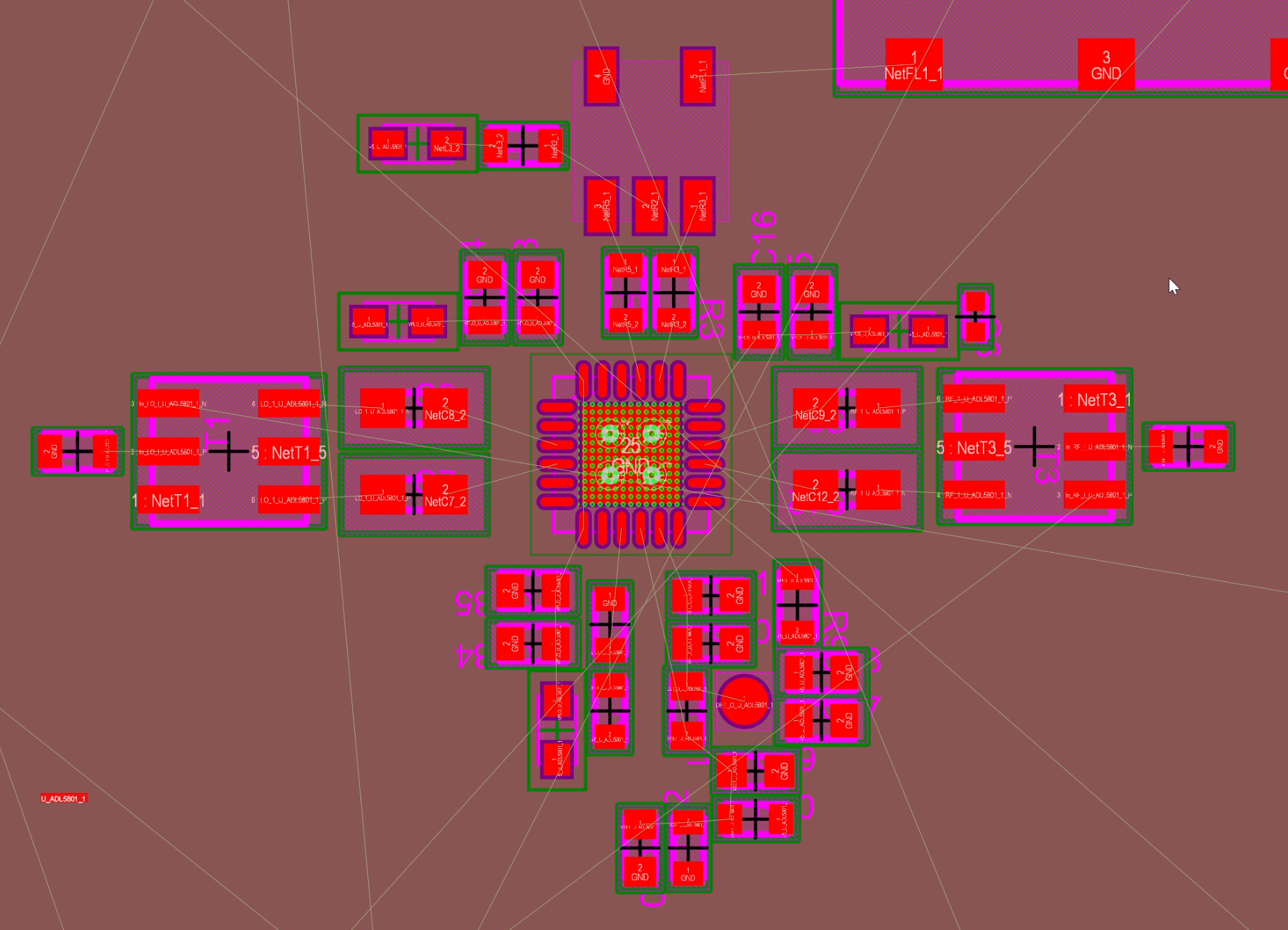
As usual, the decoupling capacitors go as close to the power pins as possible. The lowest capacitance goes closest to the IC pin. That’s to prevent any high-frequency noise from travelling too far on the power lines.
Finally, to set everything right, I rotate the whole assembly by 180 degrees to orient the connectors correctly to match the design requirements.
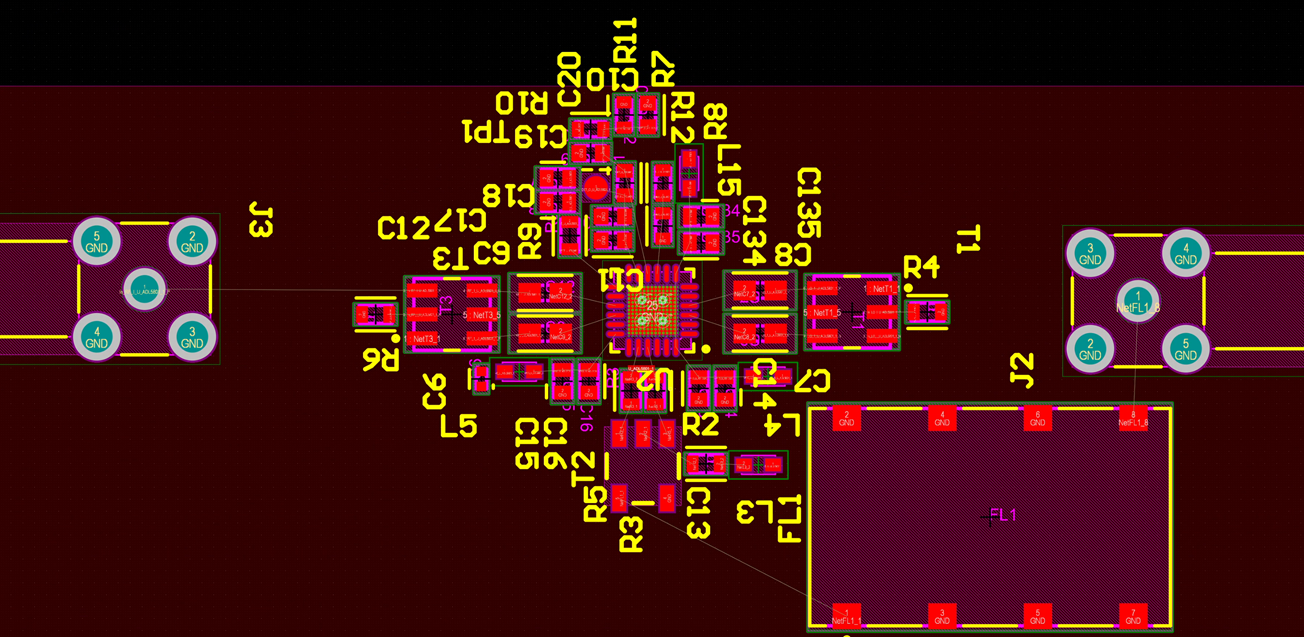
The text placement here is horrible but I won’t be using silkscreen for this particular board. I ignore the silkscreen for now and if I ever feel like adding it back, I might rearrange the text later.
Routing
The RF nets get the first preference while routing. The RF nets are critical and can’t jump around layers like other non-RF nets. Therefore, those nets must be routed first and the non-RF later.
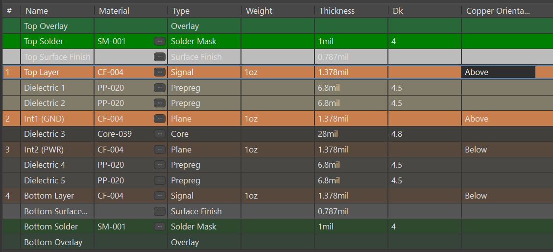
The layer stack is the most important thing to consider while routing RF PCBs. The distance between the top layer and the ground reference directly influences the trace impedance. I try to maintain a 50 Ohms impedance for the RF traces. You would see the parameter set on the high-frequency nets in the schematic. Using the parameter set, I assign the high-frequency nets to a RFCPW net class on which I would apply special rules. These special rules would assign a fixed clearance from the ground and a fixed width of the trace. Both parameters will help us achieve a 50 Ohms impedance for RF nets.
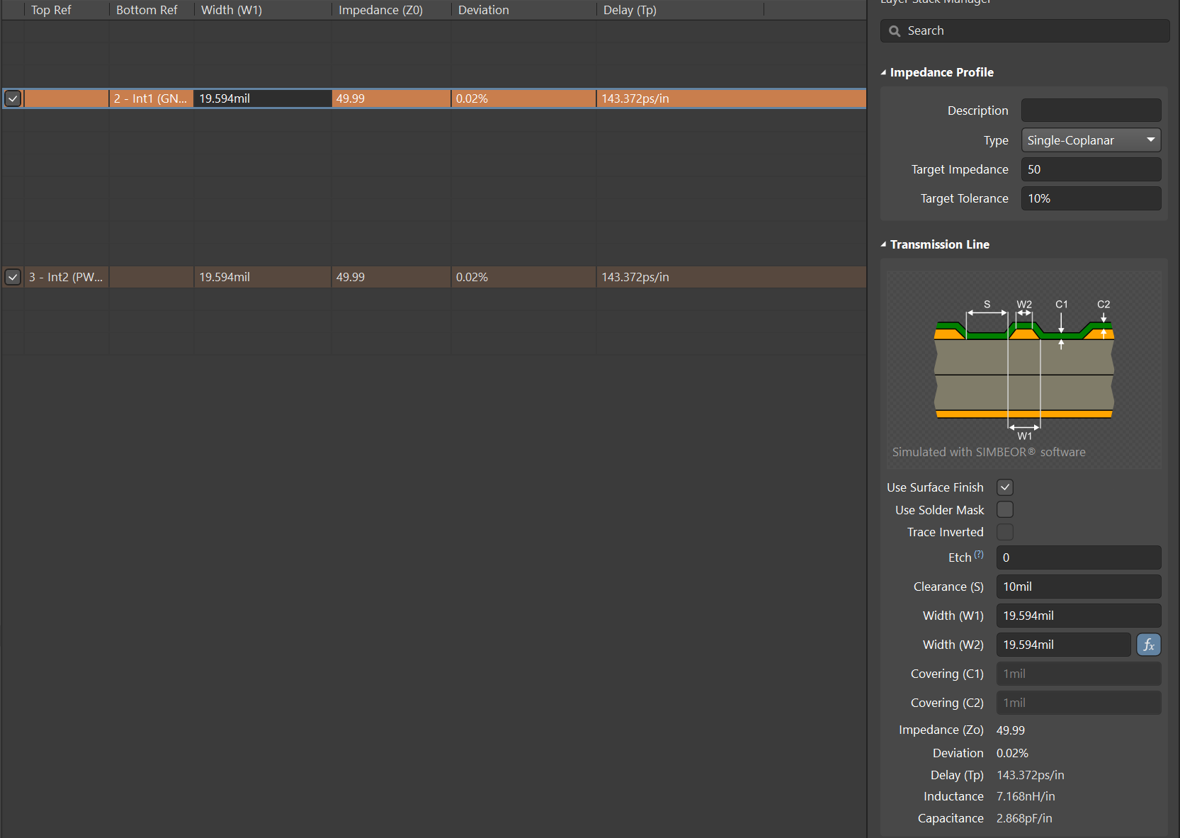
I chose to use the co-planar waveguide option for drawing high-frequency traces. In the properties, I set the clearance of 10 mills and an impedance of 50 Ohms. Based on these two inputs, Altium automatically calculates the trace width necessary to achieve the necessary impedance. There is a whole video that elaborates on this process in case you are interested.
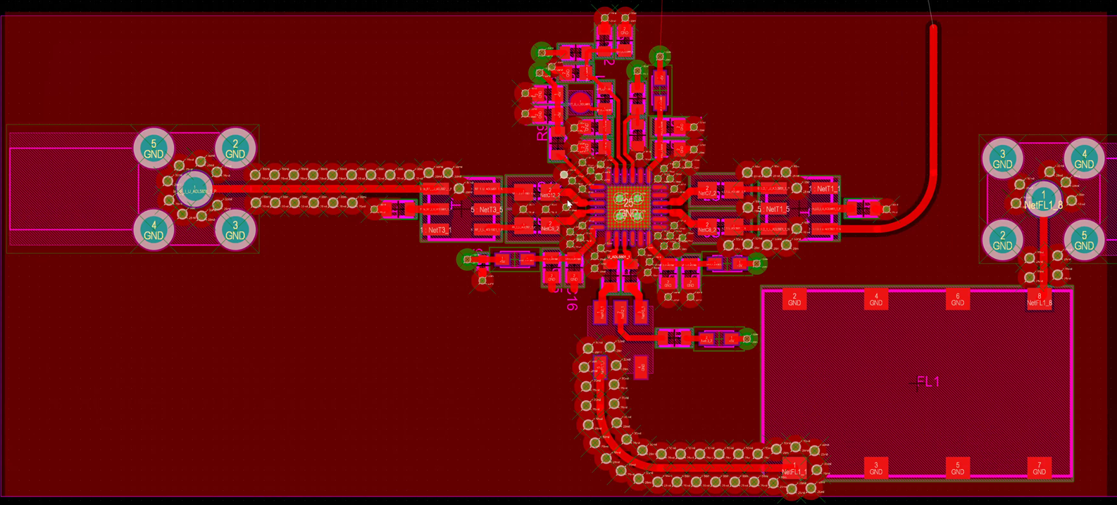
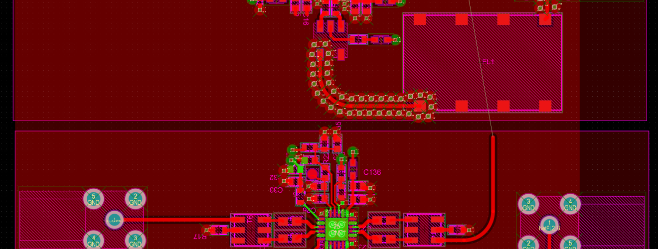
The final layout looks something like this. Being a coplanar waveguide, there’s some via shielding along the transmission lines. Additionally, I made sure to add plenty of vias around the mixer chip for low impedance connection to the ground.
In my experience, too little vias have resulted in impedance mismatch due to the effect of parasitics. So, a little extra vias is always better than having too few.
Copying layout to other circuits
Like I said earlier, this mixer is part of a multi-channel design which has a total of 4 mixers. Here, I laid out the circuit for 1 of 4 mixers. Fortunately, Altium Designer allows me to copy the layout format to other mixers. This is possible only when I use something known as “rooms”.
To copy the layout, do this; Design > Rooms > Copy Room format
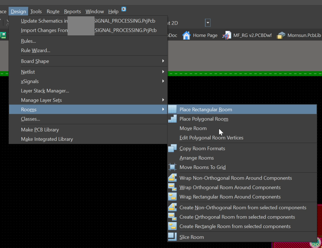
After doing this, immediately click on the room that you want to copy and then click on the room where you want to paste the copied layout.
- Click on the room you want to copy
- Click on the room where you want to paste the layout.
The result is fantastic. You save a lot of effort of placing the same circuit again and again. The room format copy feature helps you place as many identical circuits as you want. Simply put efforts in perfecting one circuit and once you are confident, copy the room format and apply the placement and layout to other identical copies.
Conclusion
To conclude, always place the critical high-frequency components first and then the low-frequency stuff. Similarly, always route the critical RF nets first and then focus on the rest. You should avoid jumping RF nets between layers to achieve an optimum impedance profile along the RF transmission line. Finally, the “copy room format” option in Altium Designer allows us to save a lot of effort when you have the same circuit repeating multiple times.

Superb….