Designing and testing a low-noise amplifier – Part 2
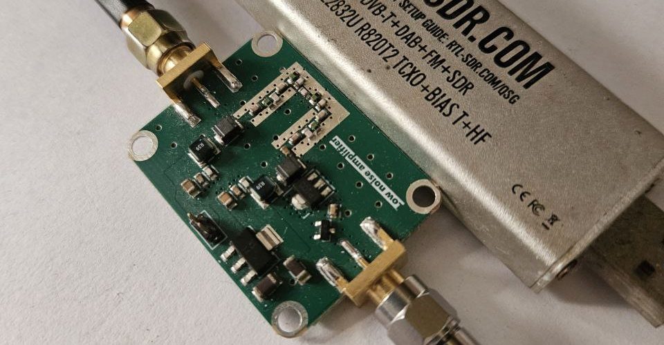
In the last post, I explained my thought process behind designing the low-noise amplifier around the PGA-103+ chip from Minicircuits. I started with defining the specifications, converting those into the schematic, making the PCB design and so on. Finally, I got it fabricated and assembled from JLCPCB. This blog post delves into the complete testing process using hobby-grade instruments. The indispensable tools for your home lab are the NanoVNA and the TinySA Ultra. These affordable devices equip you to design and test RF circuits effectively within the 5-6GHz range.
Long time ago, I posted about how NanoVNA compares to the Keysight’s N9952A vector network analyzer. We all saw the striking performance of the NanoVNA in its operating frequency range. I have no doubts on its performance. The results that I post here are quite accurate to trust the circuit for professional use. For some measurements, TinySA Ultra comes to use.
Test plan
Before we dive into testing the low-noise amplifier, lets prepare a test plan. A test plan allows us to systematically test and produce required results. In cases, you have too many parameters to test, a test plan definitely keep things organized.
The following table lists the tests carried out and the instrument used for the given test.
| Test number | Test | Instrument |
|---|---|---|
| 1 | Frequency response (Pass band insertion loss, stop band attenuation, 3dB Bandwidth, input reflection coefficient) | NanoVNA v2 |
| 2 | Input voltage range | NanoVNA v2 and variable power supply |
| 3 | Noise figure | TinySA ultra |
| 4 | RTL SDR bias Tee | RTL SDR v3 |
The first test comprises of the general frequency response of the DUT. By simply looking at the input reflection coefficient and the forward gain we get to know the overall performance of the low-noise amplifier.
In the second test, I would sweep the supply voltage from 5V to 12V to see if it causes any noticeable difference on the frequency response. The regulator that powers the LNA should ensure that the behaviour remains constant across the input voltage range.
The third test involves the tinySA Ultra to measure the noise figure of the device. This parameter tells us how much noise power the DUT adds to the input signal. A lower noise figure improves the sensitivity of the receiver.
Finally, once my low-noise amplifier passes through all these tests, I connect it to the RTL-SDR and power it up through its bias-tee. A configuration like this will allow us to use this LNA for receiving weather satellite LRPT signals without needing any additional power supply.
S-Parameter test for Frequency response
Let’s understand the test setup for measuring the frequency response of our low noise amplifier.
As explained in the Part 1, we will require bias-tee to power up the amplifier circuit.

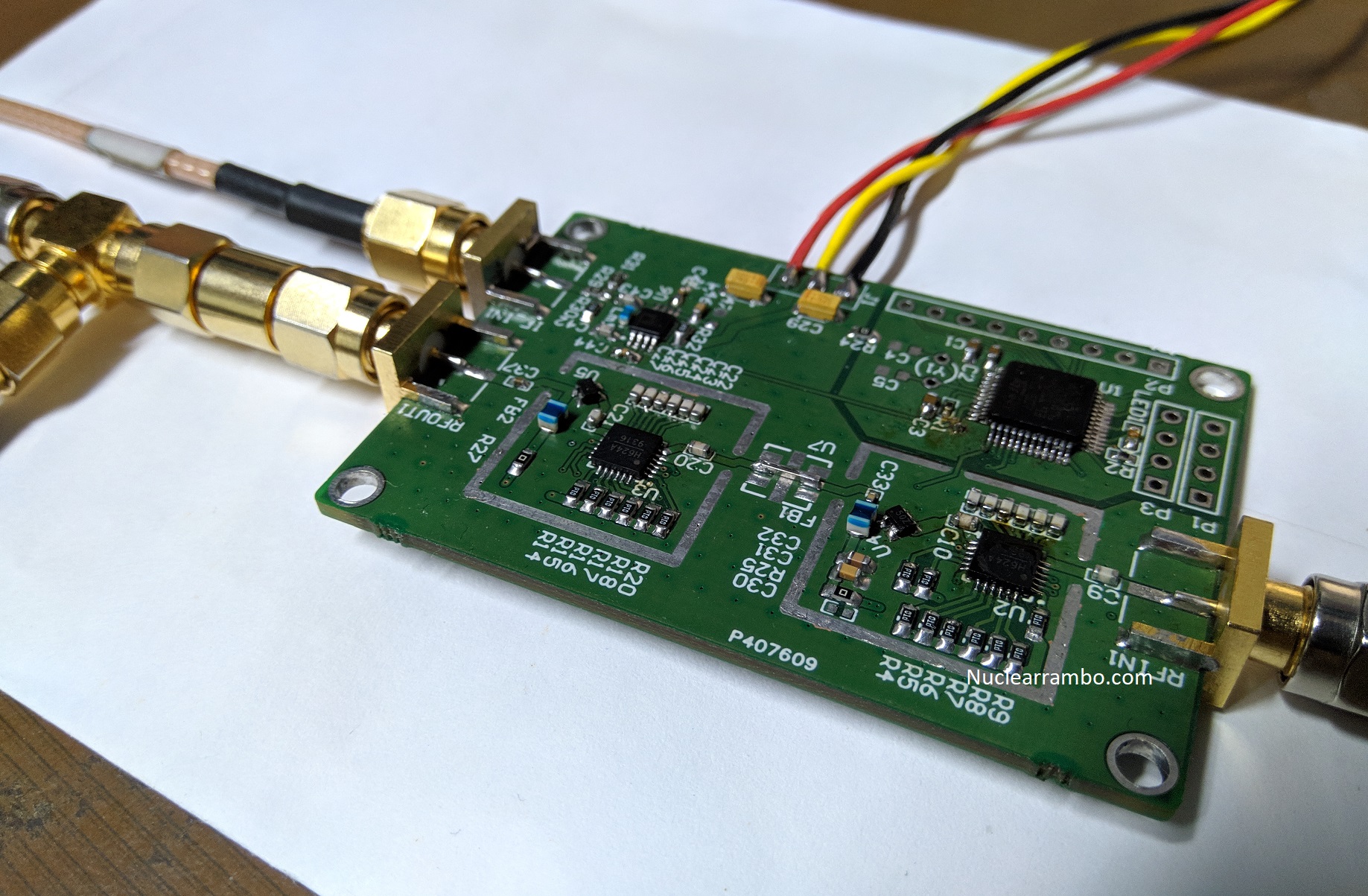
Here, I inject the DC using one bias tee which I already have in my lab inventory. Look at the image below to understand my exact setup.
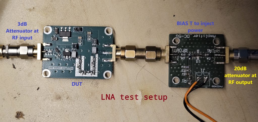
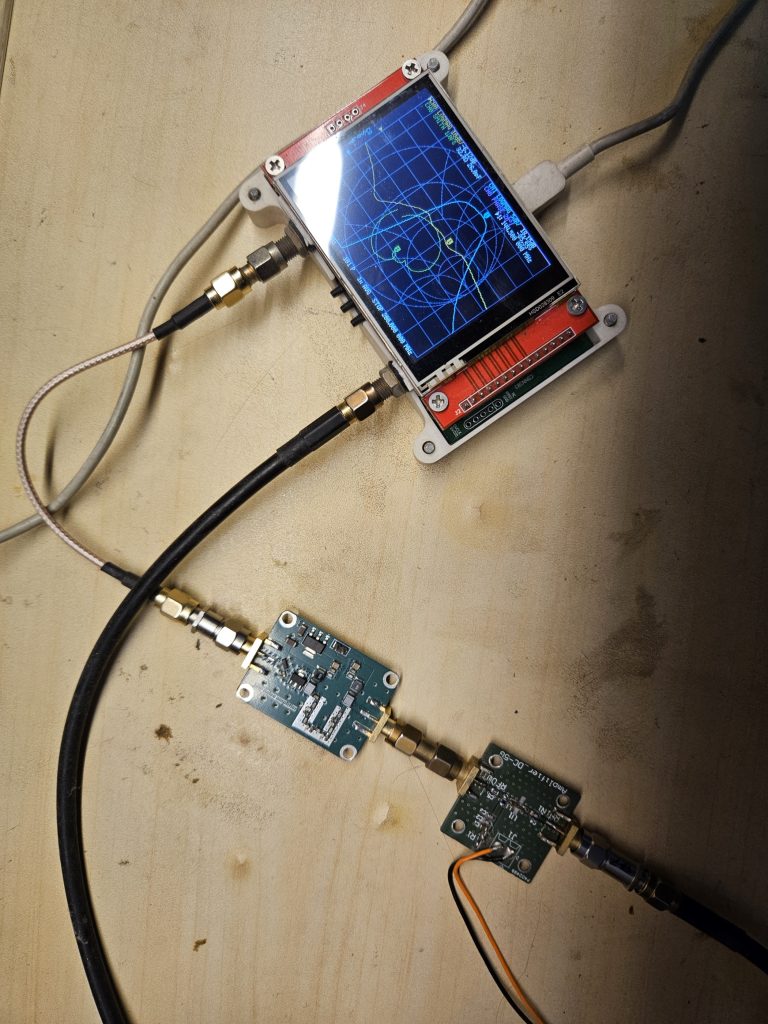
I attached a 3dB attenuator at the LNA input which may not be necessary. This port will only see RF input coming in. On the other end of the LNA board, it sees the DC power coming in while it pushes out amplified RF signal. The DC power is injected using the Bias T circuit on the right. Finally, a 20dB attenuator at the output ensures we never overload the network analyzer.
I calibrated the NanoVNA v2 with the 3dB attenuator and 20dB attenuator to compensate for the losses they would introduce in my setup. In doing so, I would be assessing solely the performance of the LNA and the Bias T circuit combined. The bias tee losses have already been measured, amounting to roughly 0.5dB to 1dB.
Let’s view the results.
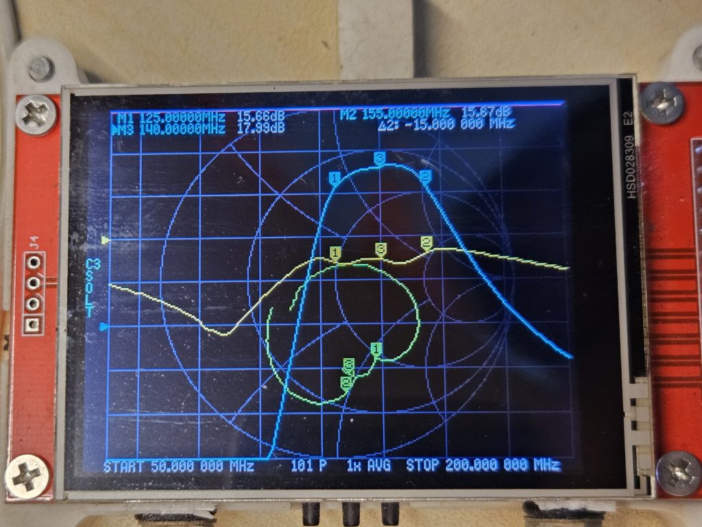
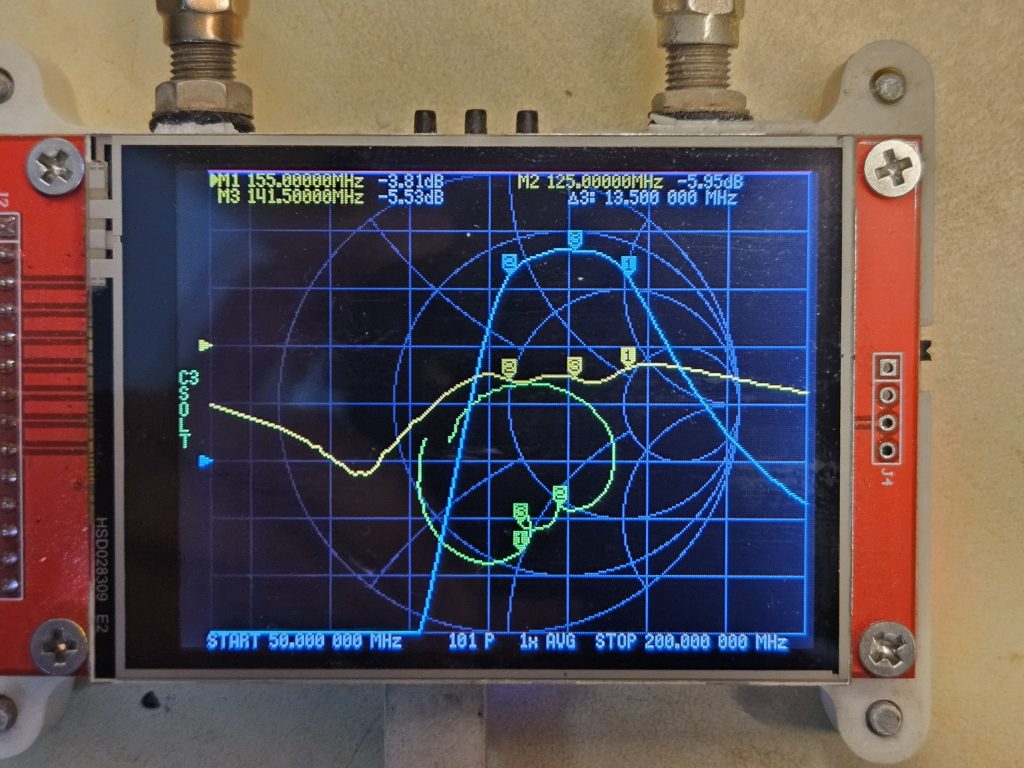
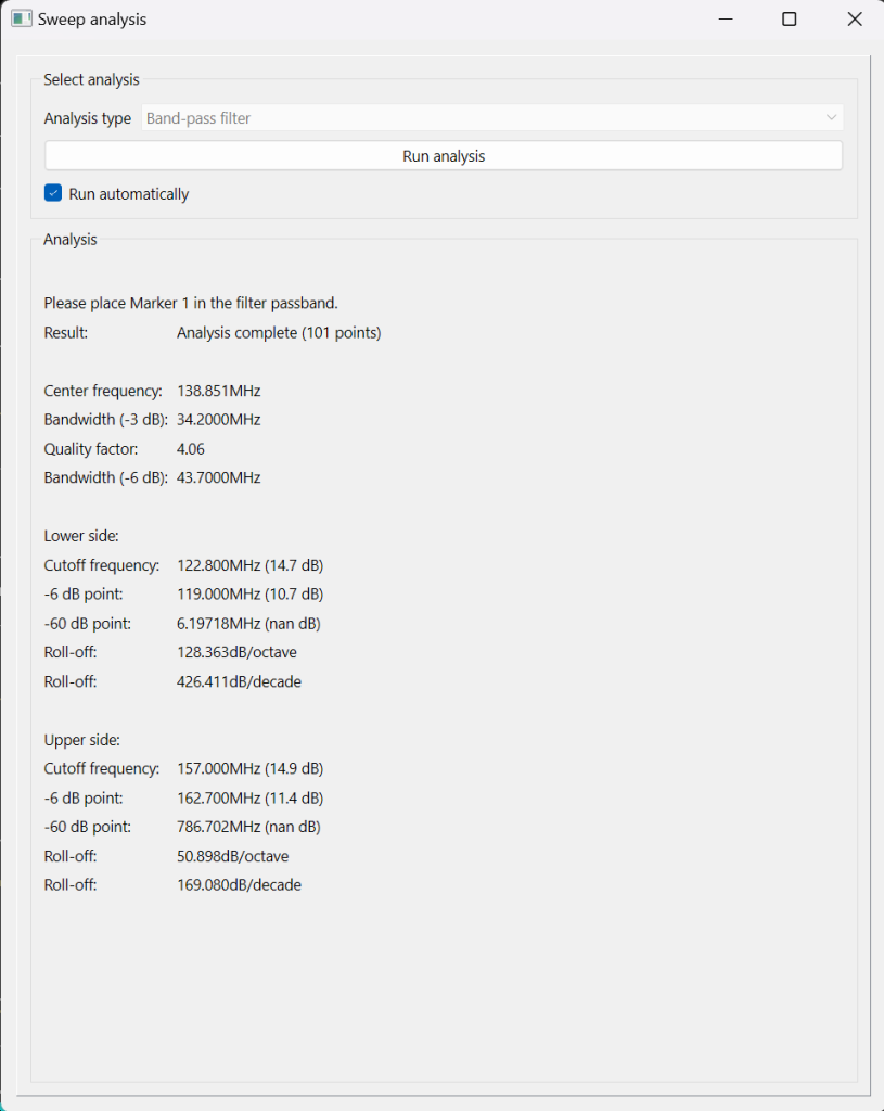
NanoVNA Saver, the open-source software that connects to NanoVNA computes the bandpass filter characteristics and presents it nicely as shown above. The bandpass filter has a -3dB bandwidth of 122.8MHz to 157MHz. This is pretty close to the theoretical computation. Furthermore, the forward gain measures to be approximately 18.2dB. The PGA-103+ datasheet shows a maximum gain of 22dB. Going by that figure, the bandpass filter must be introducing around 3dB loss.
The lower stop band shows a nice attenuation of >60dB and a sharp roll-off of 129dB/octave. Whereas the higher stop band shows a comparatively gradual roll-off of 50dB/octave and a lower level of attenuation. Now, this behaviour is also identical to the theoretically measured filter.
Looking at the input reflection coefficient, we see a >10dB S11. When it comes to LNA, you may experience poor input reflection coefficient, yet the overall performance remains unaffected.
Input voltage sweep
Having a regulator in circuit ensures the LNA is always optimally biased. This test was quite simple and all I had to do was vary the input voltage from 5V to 12V.
The regulator being well within the input voltage range ensured fixed output voltage to the LNA and the performance remained unchanged throughout.
Noise figure test
I used the tinySA Ultra to test the noise figure of the low noise amplifier. A while ago, I wrote an article about measuring the noise figure using tinySA ultra. On the other hand, if you happen to have a better spectrum analyzer, you can also read about the “Gain method of noise figure measurement” which I wrote a long ago.
Compared to the earlier setup consisting of NanoVNA v2, we use the tinySA ultra to measure the noise figure. Additionally, you require a 50 Ohms termination during the testing.
The procedure remains quite simple.
- Measure the TinySA Ultra noise figure
- Store the measured noise figure in instrument memory
- Connect the DUT and power it on
- Enter the DUT gain
- You get the result
The TinySA ultra automatically subtracts the device noise figure and the DUT gain. Whatever remains is your noise figure number.
In this case, the LNA has a gain of 18.2dB approximately. Furthermore, we are measuring the noise figure at 145MHz. Finally, we get the noise figure measurement of 0.5. The measurement is quite accurate and identical to the numbers reported by the datasheet.
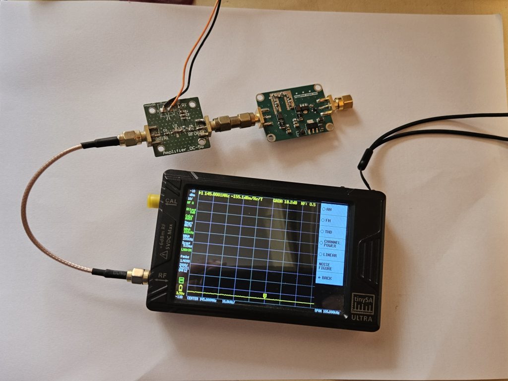
Overall, I am quite satisfied with the measurement results.
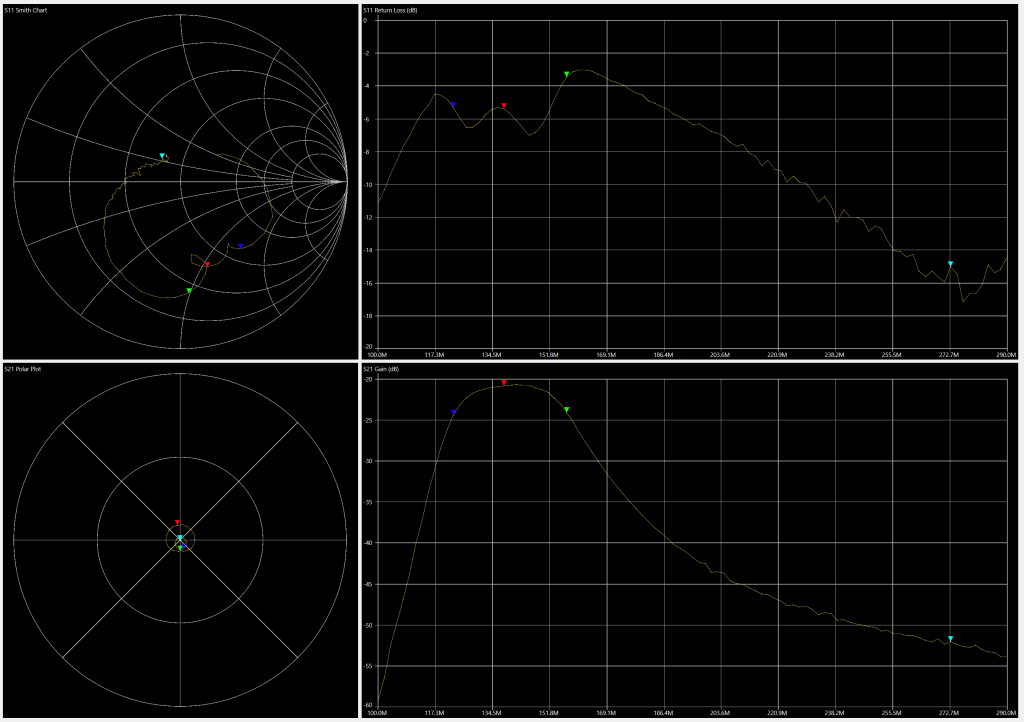
RTL SDR Test
This test is quite simple. I connected the LNA output directly to the RTL-SDR and fired up SDRAngel software to play around. As far as I know, SDR# does not have the option to enable RTL-SDR’s internal bias-tee to power up external amplifiers. On the other hand, SDRConsole, SDRAngel, both allow you to control the bias-tee.
I configured my NanoVNA in CW mode. This mode generates a fixed frequency output that one can use for testing circuits and what not. In this case, my NanoVNA is set to generate a fixed 145MHz signal that is fed into my LNA through a 3dB attenuator. First, I keep the bias-tee off and measure the signal levels which can be seen below. Also, note that I have turned off all the RTL’s internal AGCs and amplifiers.
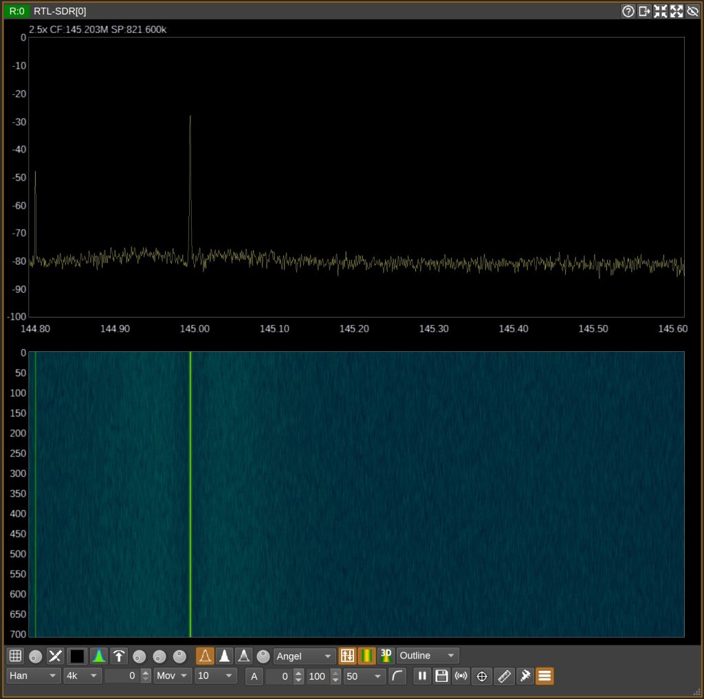
Here, the noise levels are around -80dBm while the signal peak around -26dBm.
Now, let’s fire up the RTL-SDR’s bias tee. This should supply power to our LNA and it should start amplifying the input signals.
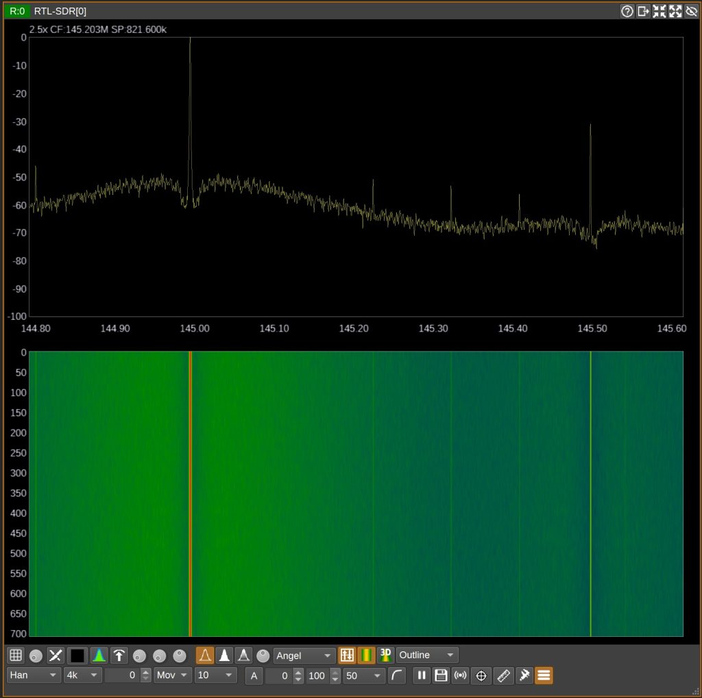
Immediately, the noise floor jumps by ~20dB and because of excess power, we see intermodulation products getting generated. Anyway, this proves that the LNA operates according to the design without any problems.
Conclusion
We began with a list of specifications, drew up schematics, and implemented the design on a PCB. To get it fabricated, we created a bunch of documentation for the fabricator. Finally, we ended up with an assembled and fully working circuit that you can use for several interesting RF projects. In this article, we learned to specify a series of tests and carry them out to confirm that our circuit is indeed working. The low noise amplifier isn’t a complicated design, but it takes quite some effort to design, assemble, define tests, and actually conduct tests to prove it’s working according to the design.
It’s been a fulfilling journey for me, and I hope you enjoyed reading this through. After going through all this, I ended up with tens of LNA boards—a lot more than I could use. So, if you wish to purchase them, contact me in the comments below.
I also ended up creating my first datasheet.


I am interested in this LNA but for other frequencies, do you do customizations?