
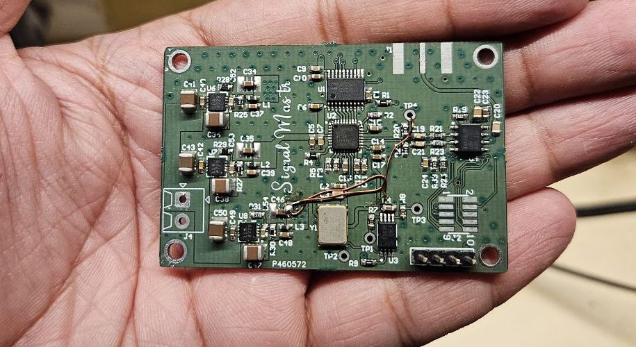
DIY STM32 and AD9913 signal generator board
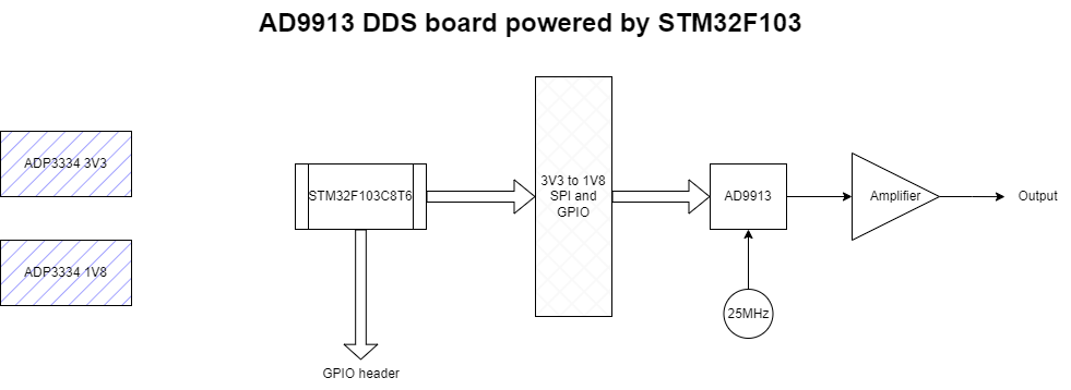
The AD9913 direct digital synthesizer works as a digital waveform synthesizer that can generate signals with very precise resolution. When it comes to radio receivers, the AD9913 with <0.05Hz resolution can be used as a beat frequency oscillator for SSB demodulation. As compared to the AD9833 DDS, the AD9913 has an internal PLL that can internally generate higher sampling rates. This allows us to use a lower-frequency external oscillator. Additionally, the AD9913 is a very low power chip, and it takes very little power. Therefore, this chip generates very little heat.
This circuit generates clean sine wave signals or it may also generate signals based on a frequency ramp profile. ‘Frequency profile’ is a very good feature when it comes to generating any frequency varying waveforms. Additionally, frequency profiles can also allow frequency hopping often used in wireless communication systems. The DDS finds itself in many applications but we won’t dive into those in this article. The main purpose of this article is to show the board design and a basic firmware that is able to generate any frequency in the given limits. The article does not go too deep into the theory. I have simply attempted to demonstrate the “top level” working of this board with a few tips here and there to get your design working.
The schematic
The hardware is designed with help of the reference design provided by Analog devices. It uses three linear voltage regulators: one for powering the microcontroller, one for analog signal conditioning and one for the digital signals controlling the DDS. I could have used a signal regulator for the DDS but I went for three for keeping the output signal generation noise free.
The power section
As described above, I used 3 voltage regulators with 2.6V to 11V input range with part number ADP3334. Although quite expensive, I wanted to consume the stock of these regulators that I already own. Feedback resistors at the output set the output voltage of the regulator.
You can either calculate the feedback resistor network on your own or refer the datasheet and use the suggested values.
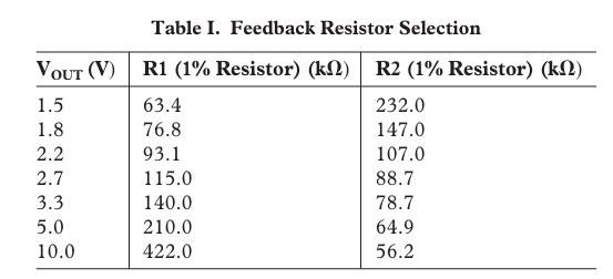
I went the easy route and used the suggested resistor values and design my schematic as shown below.
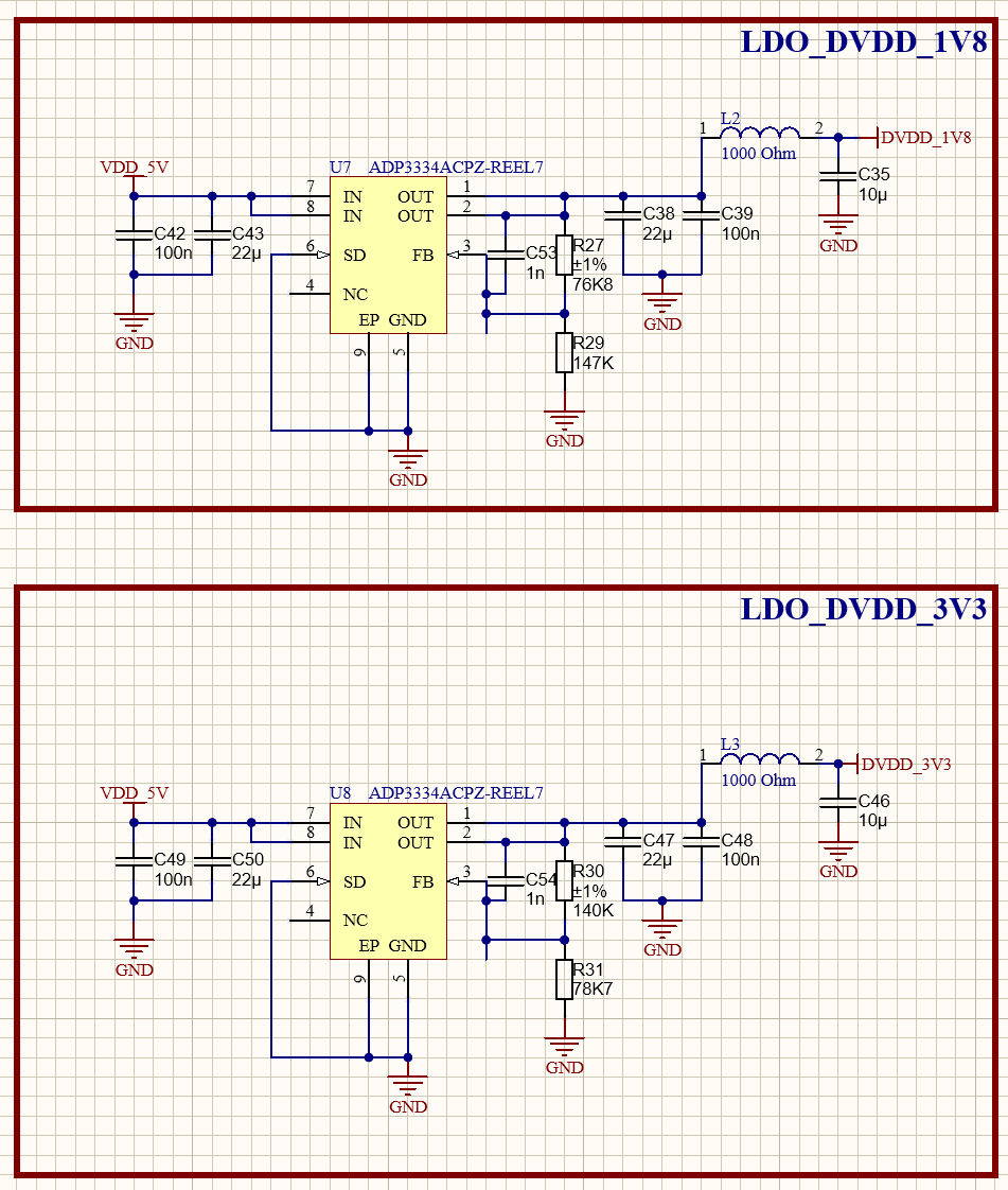
The simplest schematic suggested by Analog devices allows you to skip the input capacitors and only have a single 1uF capacitor at the output. For better noise rejection and stability, I chose to add the input and output capacitors. Additionally, I also added a LC filter at the output for further noise filtering. Based on your choice, you can decide to bypass it with a 0 Ohm resistor.
There is another regulator that generates analog 1V8 supply for the DDS core and that’s not shown here.
Microcontroller
The STM32F103C8T6 might be one of the most used microcontrollers in my projects. As a result, it became the controller of my choice for this project. It’s definitely an overkill of a microcontroller for this project but its already quite inexpensive, so who cares?
The STM32F103C8T6 is powered by a 3V3 supply generated by the ADP3334 regulator we discussed above. I brought out the SPI port and a few GPIO pins that control the AD9913 DDS. Additionally, I also brought out spare GPIO pins on an SMD header which may come handy when I am using this board for a more complex project. I also brought out the SWD port on a 4 pin header useful for programming the controller. Apart from the interfaces, each power pin has a couple of decoupling capacitors for noise filtering.
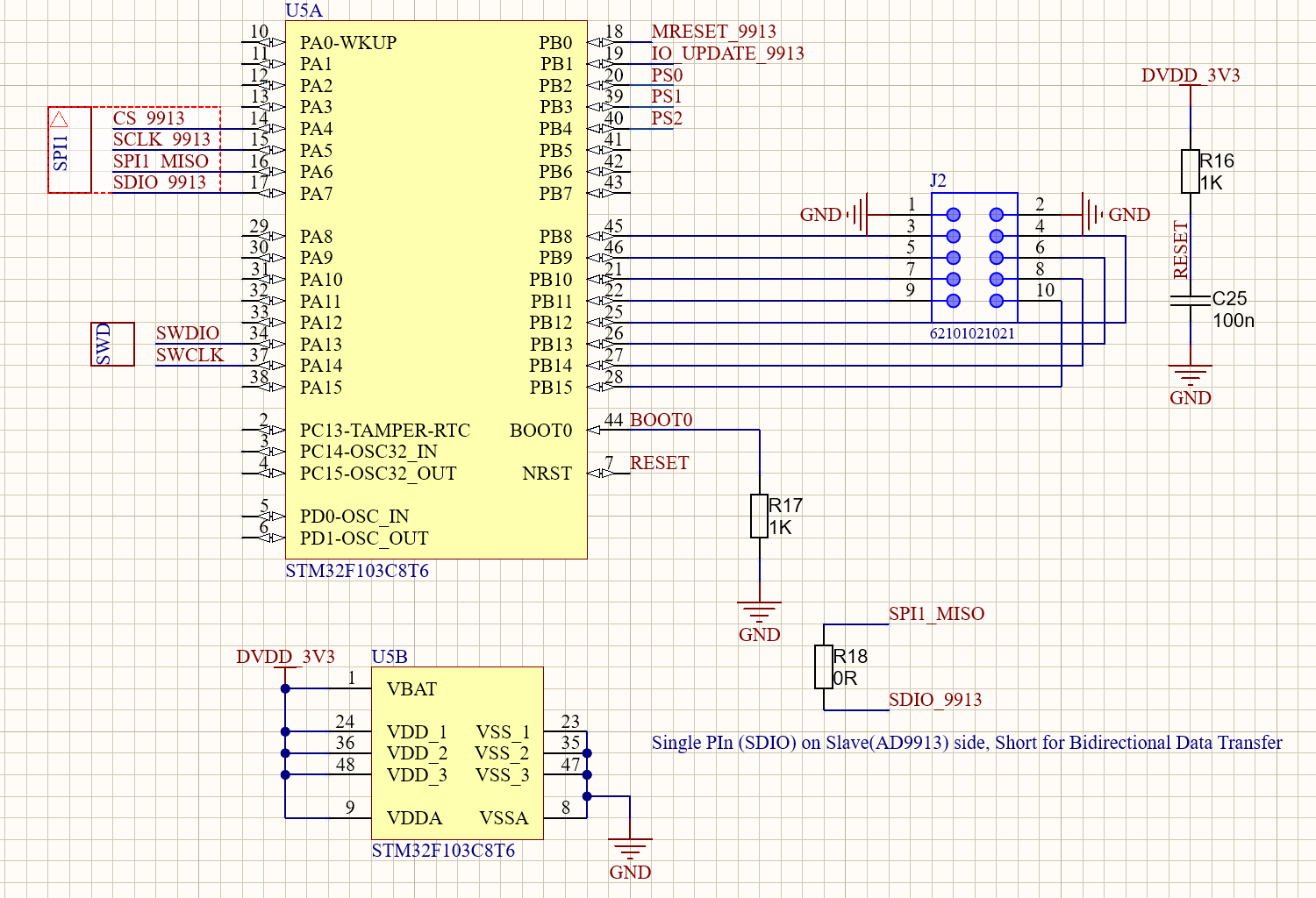
An additional level translator is needed for connecting the controller with the AD9913. The level translator converts 3V3 signals from the microcontroller to 1V8 level required by the DDS.
Before we look at the AD9913 schematic, lets have a quick look at the clocking section.
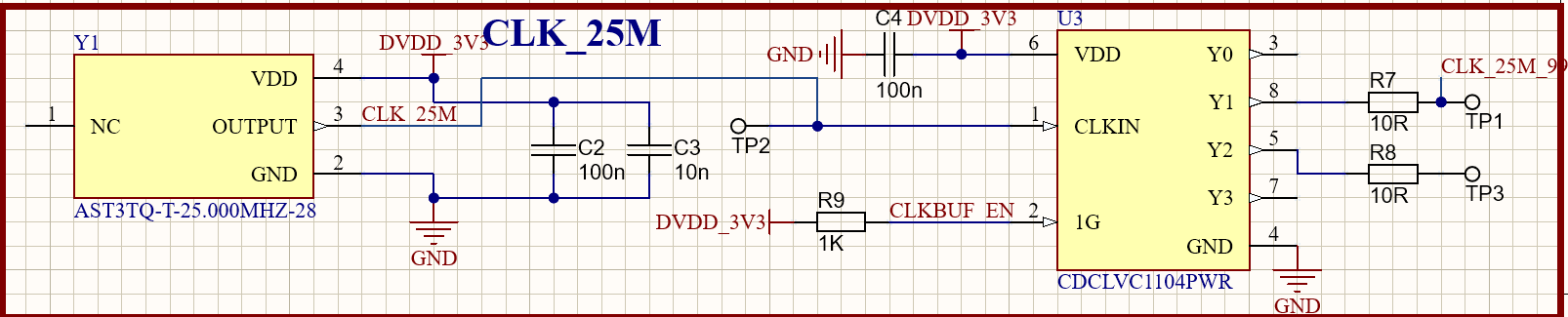
For best frequency stability, AST3TQ-T-25.000MHz-28 works out to be the best. It has an initial frequency tolerance of 0.3ppm and a +280ppb stability across the industrial temperature range. Now, to have such nice stability also requires a lot of money. For general use, you could go with something like CWX823-25.00 TCXO.
Clocking
The AD9913 DDS can be clocked both ways, single ended or differential. Apparently, there appears to be no problem with either approach. Nevertheless, I included a transformer for single ended to differential conversion whose footprint went wrong in the first version, and I had to flip the part 90 degrees while soldering it.
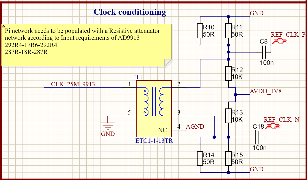
Prior to this conversion, I have an additional clock buffer CDCLVC1104PWR that takes TCXO signal and splits out into 4 buffered clock outputs. In case you wish to use the same TCXO and synchronize other modules, you can pull out the buffered output and connect that to other modules.
Output conditioning
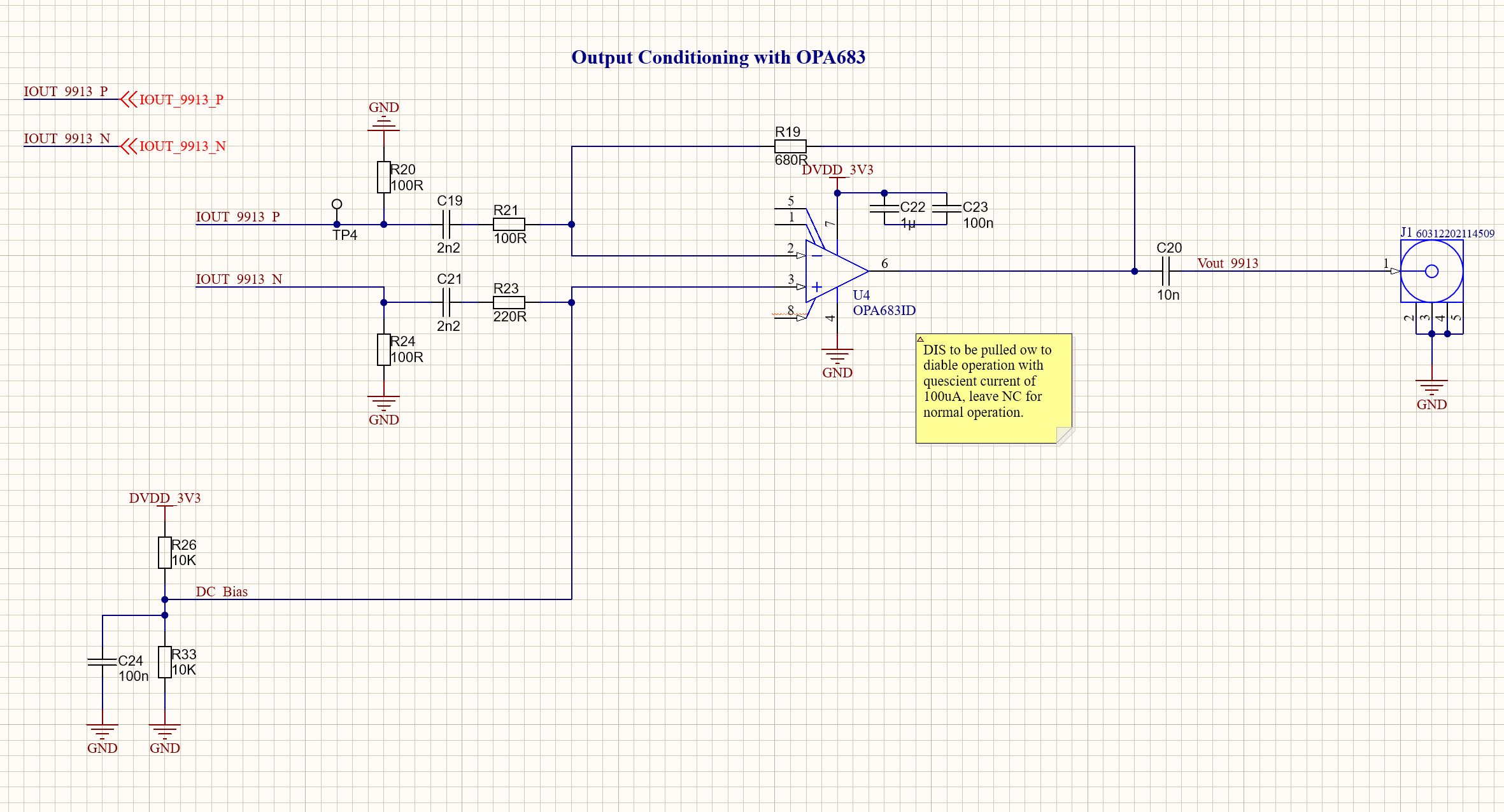
The AD9913 DDS produces differential output. I used OPA683 operational amplifier to convert this differential signal to single ended output. Furthermore, I have also configured the circuit to block DC on the inputs and output.
Now that we are done understanding the hardware schematic, lets move on to the firmware section.
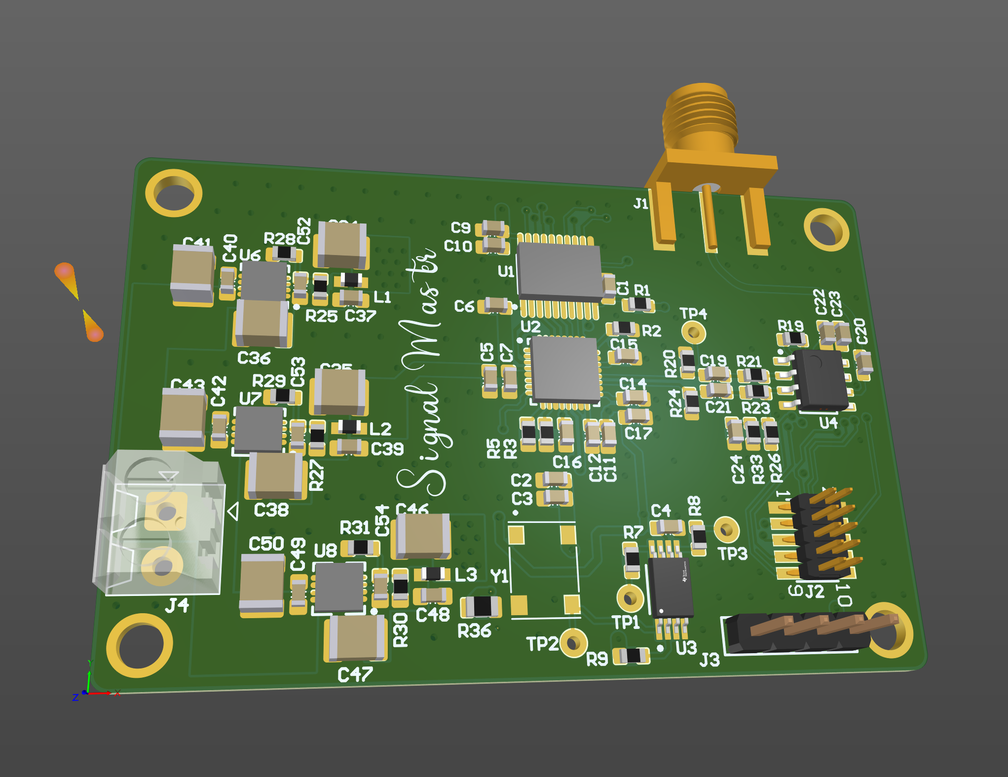
The PCB Layout
I did the PCB layout in Altium Designer. Here, I started by placing the regulator section first. Referring to the recommendations provided by the chip manufacturer guarantees better chances of your design working in the first attempt.
Also, before starting any PCB layout, I ensure to set my PCB stack up properly. I used a 4-layer stackup with first layer for signals, second layer for ground, third layer for power and the fourth layer for general signal routing.
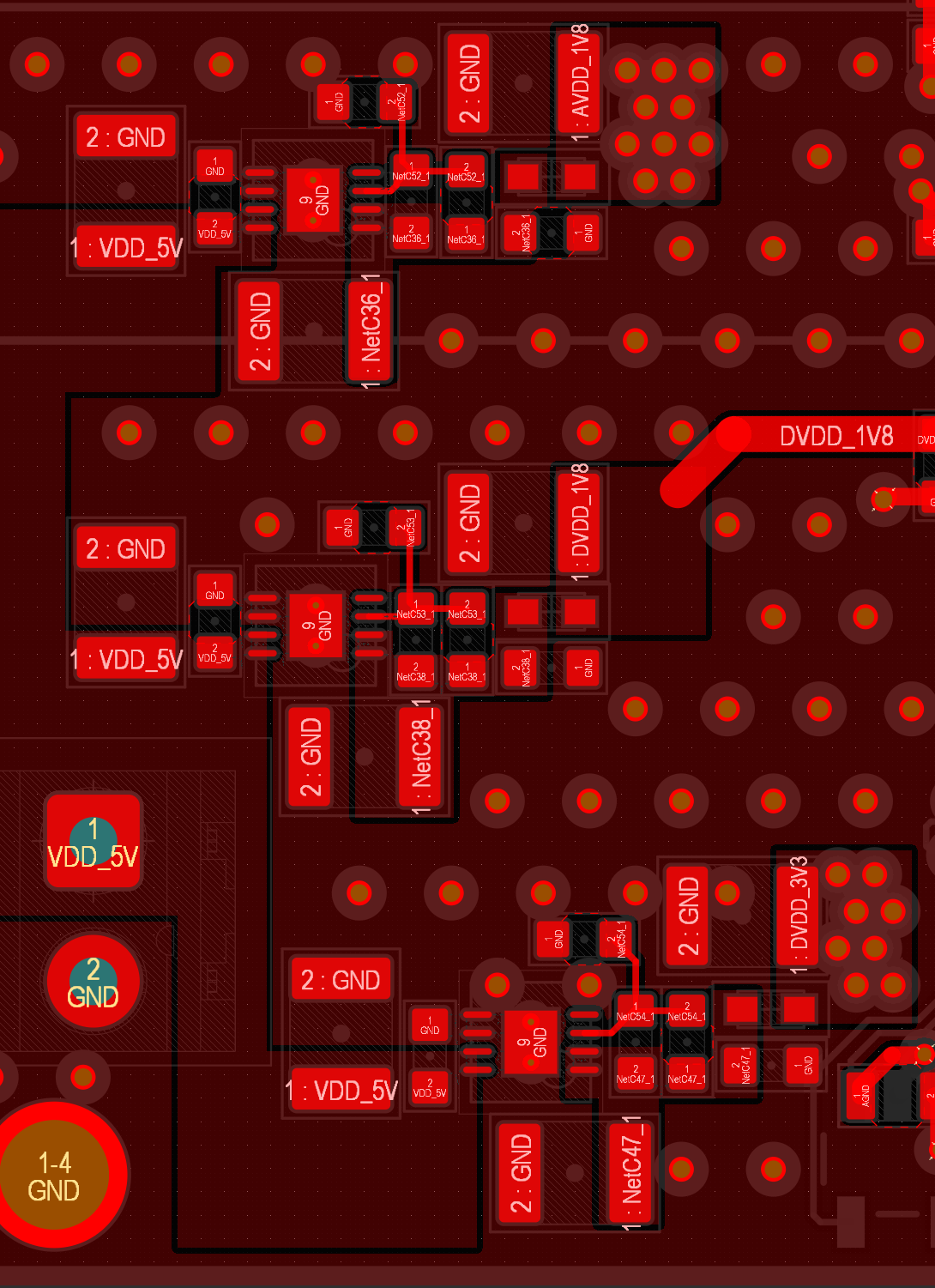
When layout the regulator section, I tried keeping the decoupling capacitors and filters closer together to ensure minimum noise pickup a small ground loops. Since, this board is a 4 layer board, I routed certain power rails from the 3rd layer.
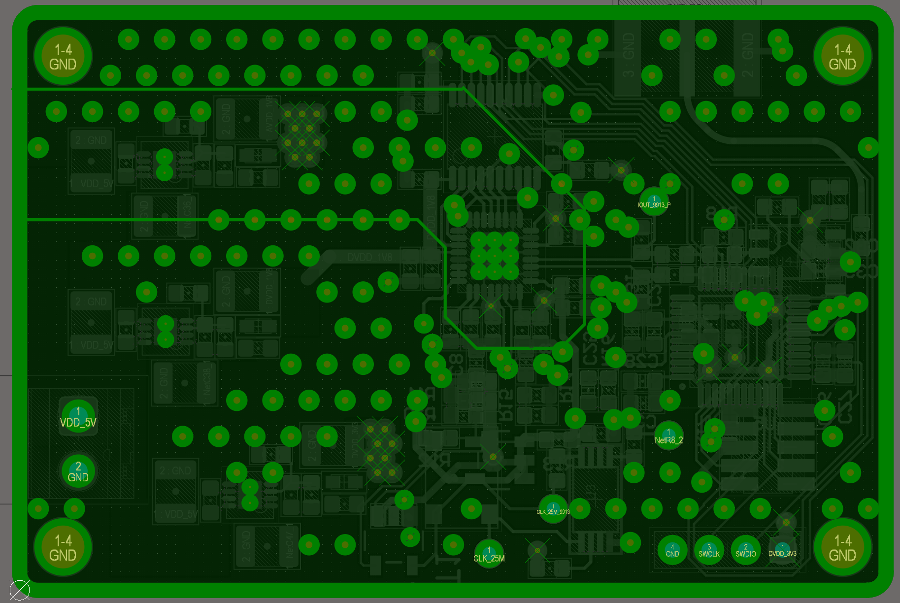
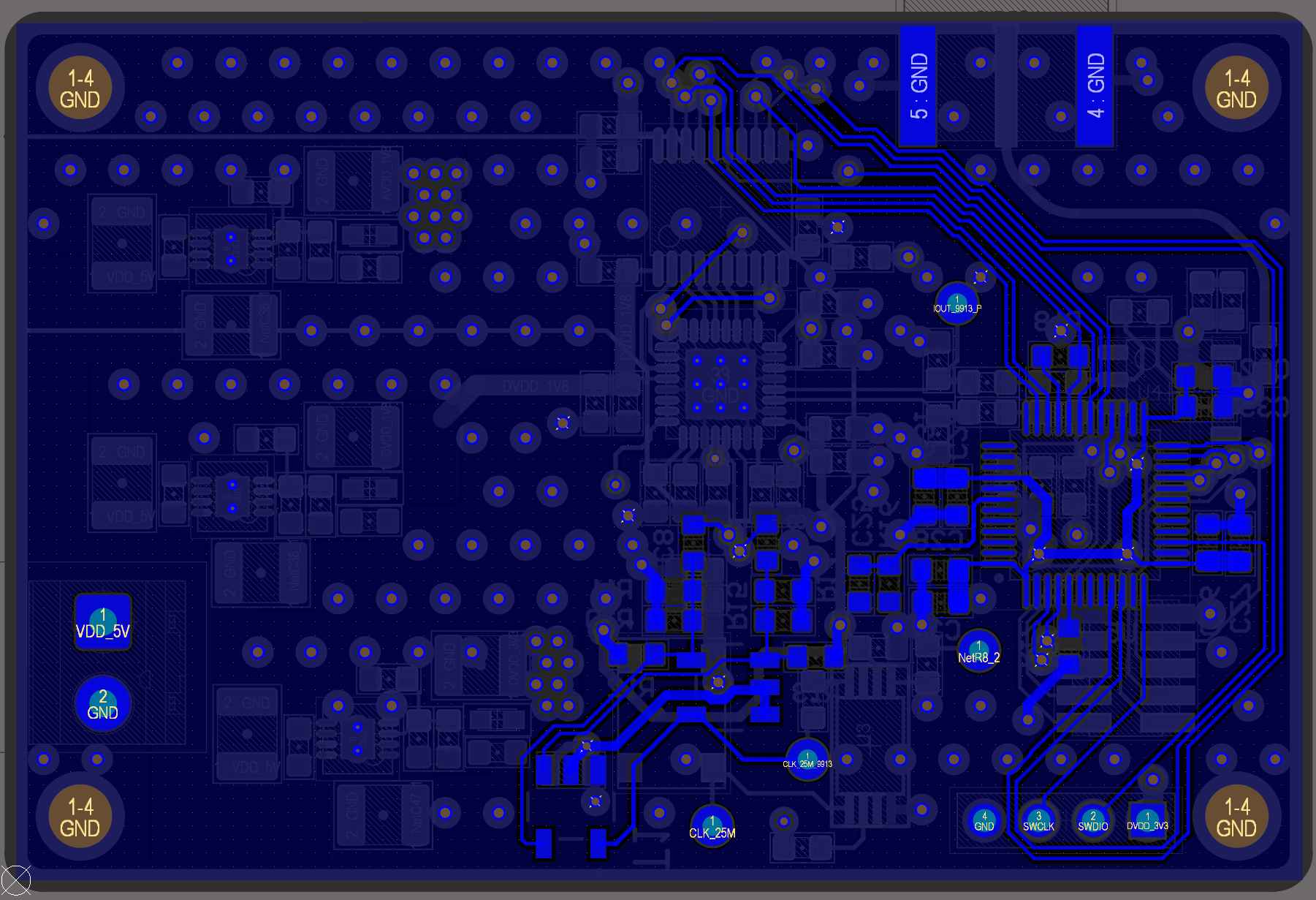
The microcontroller and its decoupling capacitors went down on the bottom layer.
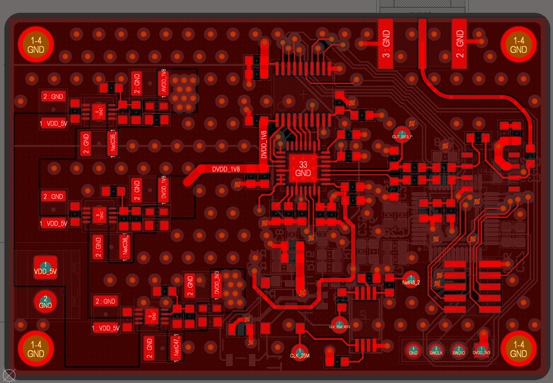
Observe carefully, how the power traces are thicker than the other signal tracks. This is to ensure low impedance power path.
Additionally, also observe the copper under the capacitors has been removed to reduce all parasitic capacitances. Finally, the output signal is drawn out from an SMA connector on the edge.
AD9913 DDS Firmware for STM32 microcontroller
It’s important to program the AD9913 DDS chip to make it function properly. There are a bunch of registers that set the frequency and phase of the output signal. Additionally, two configuration registers control the overall chip behaviour.
I wrote register definitions in the header file such that each bit can be configured independently. Furthermore, my easy-to-use library allows me to quickly set the output frequency. An output scaling register allows me to control the output amplitude.
|
1 |
dac_ad9913.bit.FS_C = 425; //Controls the amplitude |
To set the output frequency, call this function.
|
1 |
ftw_ad9913.bit.freq_tuning_word = AD9913_calculateFreqReg(70000000, sys_clk); |
After every SPI transaction, we need to toggle the IO_Update pin for the configuration to take effect.
|
1 |
AD9913_IO_UPDATE(IO_UPDATE_GPIO_Port, IO_UPDATE_Pin); |
The full configuration section is shown below.
|
1 2 3 4 5 6 7 8 9 10 11 12 13 14 15 16 17 18 19 20 21 22 23 24 25 26 27 28 29 30 31 32 33 34 35 36 37 38 39 40 |
HAL_GPIO_WritePin(MRESET_GPIO_Port, MRESET_Pin, GPIO_PIN_SET); HAL_Delay(1); HAL_GPIO_WritePin(MRESET_GPIO_Port, MRESET_Pin, GPIO_PIN_RESET); cfr1_ad9913.reg = 0x00000000; cfr1_ad9913.bit.sin_out_en = 0; cfr1_ad9913.bit.sync_clk_disable = 0; dac_ad9913.reg = 0x00000000; dac_ad9913.bit.FS_C = 425; ftw_ad9913.bit.freq_tuning_word = AD9913_calculateFreqReg(70000000, sys_clk); HAL_Delay(10); AD9913_writeSPI_32bit(SPI1_CS_GPIO_Port, SPI1_CS_Pin, &hspi1, cfr1_ad9913.reg, CFR1_ADDRESS); HAL_Delay(4); AD9913_IO_UPDATE(IO_UPDATE_GPIO_Port, IO_UPDATE_Pin); cfr2_ad9913.reg = 0x00000000; cfr2_ad9913.bit.pll_pwr_down = 0; cfr2_ad9913.bit.pll_reset = 1; cfr2_ad9913.bit.pll_mul_factor = 0x0C; cfr2_ad9913.bit.pll_out_div_2 = 0; cfr2_ad9913.bit.pll_input_div_2 = 0; cfr2_ad9913.bit.vco2_sel = 0; cfr2_ad9913.bit.cmos_clk_mode = 0; cfr2_ad9913.bit.crystal_clk_mode = 0; AD9913_writeSPI_16bit(SPI1_CS_GPIO_Port, SPI1_CS_Pin, &hspi1, cfr2_ad9913.reg, CFR2_ADDRESS); HAL_Delay(4); AD9913_IO_UPDATE(IO_UPDATE_GPIO_Port, IO_UPDATE_Pin); AD9913_writeSPI_16bit(SPI1_CS_GPIO_Port, SPI1_CS_Pin, &hspi1, cfr2_ad9913.reg, CFR2_ADDRESS); HAL_Delay(4); AD9913_IO_UPDATE(IO_UPDATE_GPIO_Port, IO_UPDATE_Pin); AD9913_writeSPI_32bit(SPI1_CS_GPIO_Port, SPI1_CS_Pin, &hspi1, dac_ad9913.reg, DAC_ADDRESS); HAL_Delay(4); AD9913_IO_UPDATE(IO_UPDATE_GPIO_Port, IO_UPDATE_Pin); AD9913_writeSPI_32bit(SPI1_CS_GPIO_Port, SPI1_CS_Pin, &hspi1, ftw_ad9913.reg, FTW_ADDRESS); HAL_Delay(3); AD9913_IO_UPDATE(IO_UPDATE_GPIO_Port, IO_UPDATE_Pin); |
It’s imperative that we reset the chip using “Master reset” pin. Without the reset, the DDS exhibits very unpredictable behaviour.
Debugging
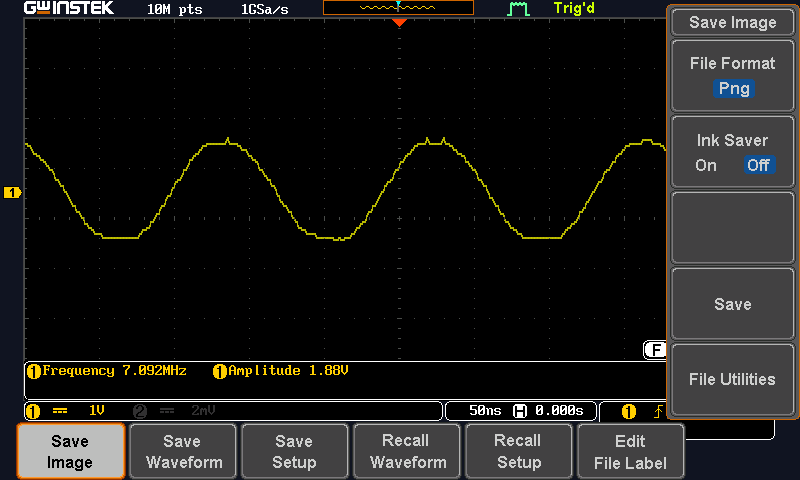
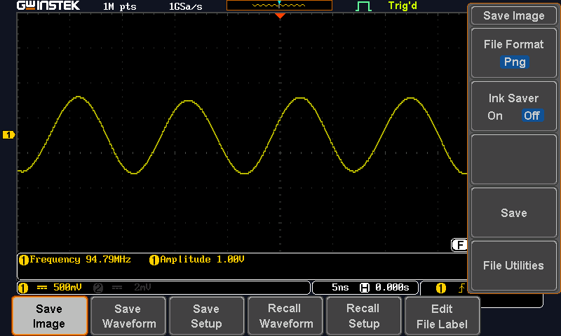
We all love a way to know if our design works correctly. Fortunately, there is one way to verify the clocking network by observing the SYNC_CLK pin of the DDS chip. It so happened in the beginning that I wasn’t able to get a signal out of the DDS. By observing if there was a signal on the SYNC_CLK I could at least verify that my board was working fine. By default, the DDS outputs a signal of the same frequency as REF_CLK. For example, if your TCXO is 25MHz, then you should be able to observe 25MHz on the SYNC_CLK pin using an oscilloscope.
Furthermore, when you program the PLL to produce, lets say, 100MHz, then your SYNC_CLK should output 100MHz.
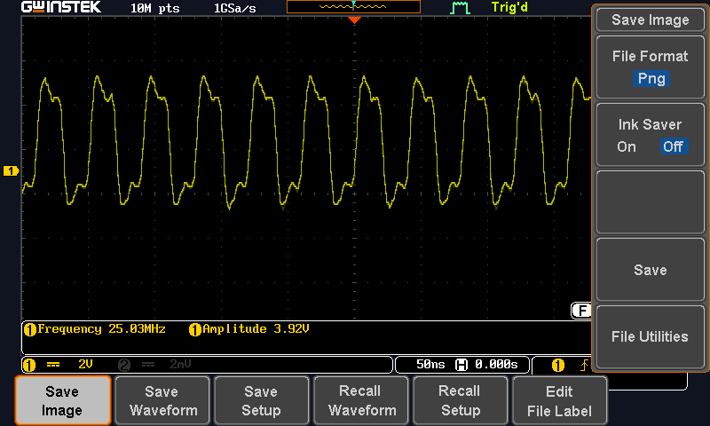
While getting my board to work, I wasn’t able to consistently produce any output on the SYNC_CLK. It was at that moment that I realized that I needed to reset the chip before programming the registers. After asserting master reset for 1 ms, and then following the configuration sequence resolved most of my problems. I could consistently program the chip and obtain the desired signal out of the DDS.
So, here are a few screenshots that demonstrate various output frequencies produced by the DDS. The true spectral purity of the DDS should be observed on a spectrum analyzer. Unfortunately, I do not have the spectrum analyzer at hand.
I will definitely post part 2 of this article where I would implement the frequency ramps, triangle output, frequency modulation, etc.
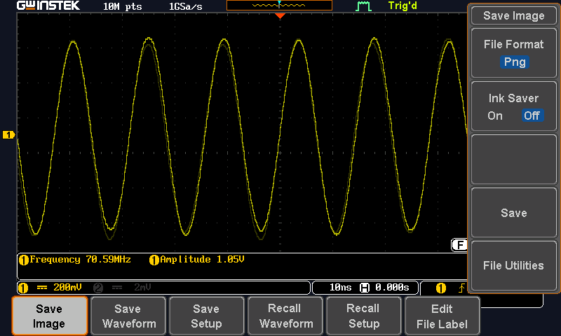
Due to the low pass response of the Opamp, I had to pump up the output scaling factor on the DDS.
Conclusion
AD9913 DDS is a very versatile DDS which could be used like a VFO in an amateur radio receiver. It could also be used for generating a frequency ramp for a stepped frequency radar. If not for anything, it could at least be used as a low-frequency signal generator on your desk.
I made a few extra boards for myself. If you happen to love the design and wish to purchase it, let me know in the email below.
Hmmm good one, though I have a question, which software you are using for this oscilloscope? Is it the Oscilloscope in Proteus ?
is it this one: https://www.theengineeringprojects.com/2013/06/how-to-use-oscilloscope-in-proteus-isis.html ?
Is it the proteus oscilloscope or you are using any other software.
again good work, keep it up.
I captured the screenshot on the GWInstek GDS1102B oscilloscope. There is no software being used here. Its a capture from the scope itself.