Manual VCO selection for a faster locking PLL
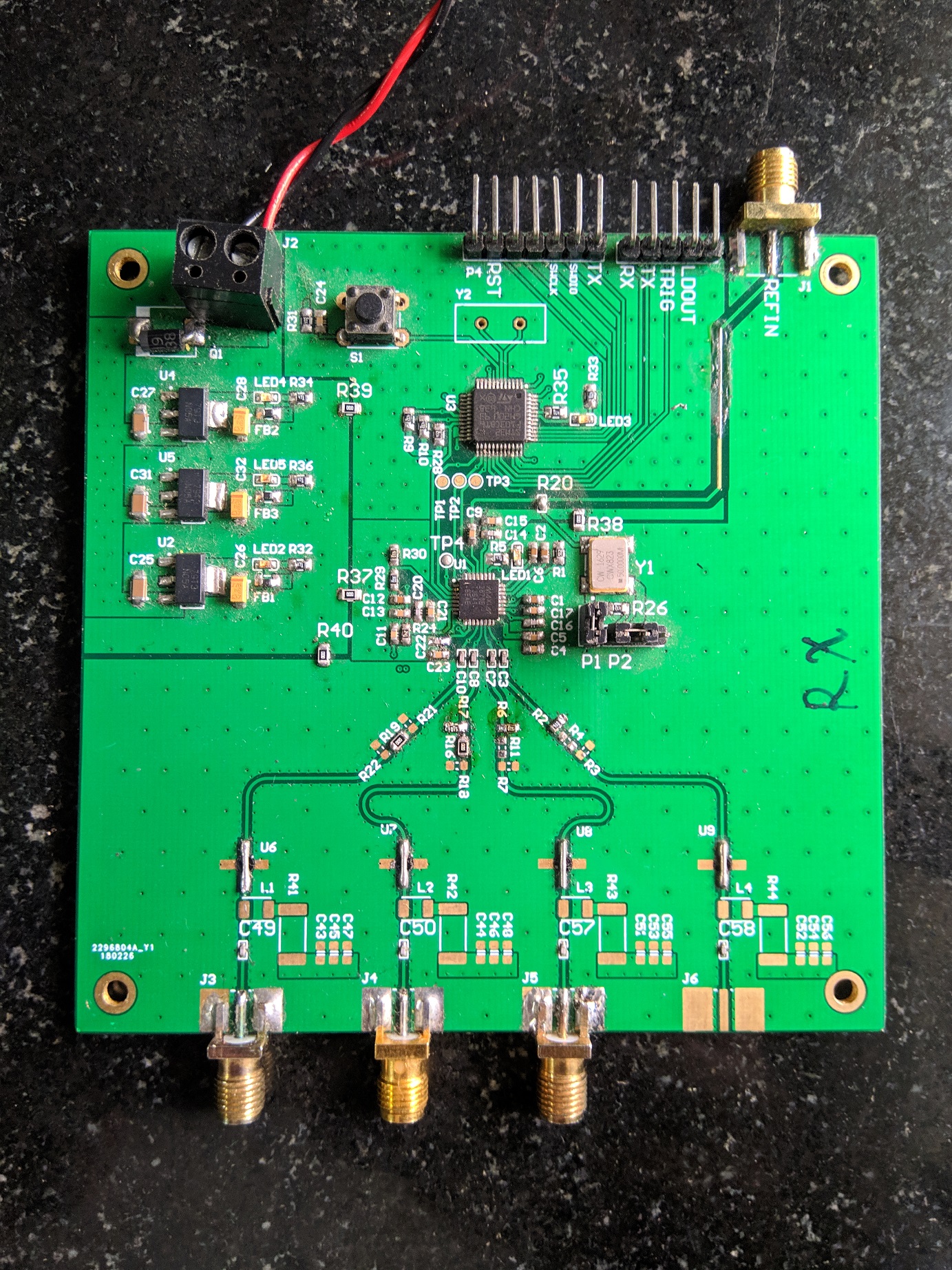
PLL chips such as the ADF43xx, MAX287x and so on come with an integrated VCO. The frequency range on these PLL chips can extend all the way from few tens of MegaHertz to several GigaHertz. Such a wide range of output frequency can be obtained only if you have a VCO that can tune over a wide range of frequencies. Let’s take an example of MAX2870 PLL which promises a tuning range from 27MHz to 6GHz. Internally, it has a continuous VCO tuning range from 3GHz to 6GHz which is further divided to obtain the lower frequencies. A single VCO that can tune over 3GHz range is quite difficult to design. Having multiple VCOs that can tune over smaller ranges solves the problem.
A little about the insides
MAX2870 PLL has 4 VCO cores with 16 sub-bands that allow continuous tuning from 3GHz to 6GHz. This gives us 64 different VCOs to choose from depending on the output frequency we desire. An internal state machine selects a VCO core and a corresponding VCO sub-band. Furthermore, the selected VCO’s tune input gets connected to the external loop filter output. The state machine in MAX2870 is clocked at mere 50kHz leading to a slower lock time. What if we were to bypass this state machine and tell the chip straight away to choose a particular VCO? In case you are using ADF4351, it lets you clock the VCO auto select state machine to a higher clock rate. I haven’t tried clocking the MAX2870 PLL’s band select clock higher than 50kHz. May be, I would try that sometime soon.
Building a register look up table
Coming back to the main point, we can manually select the VCO inside MAX2870 significantly reducing the time required to lock the PLL. Maxim Integrated Inc. claims that you can shave off approximately 200 microseconds from the lock time. The datasheet provides a basic method on how that can be achieved. For example, you have a certain frequency points that you know the PLL needs to lock on to. Firstly, enable the VCO auto-select state machine and program the PLL to your desired frequency. Secondly, readback the Register 6[8:3] and store it. Similarly, follow this procedure for all the frequency points you need. Finally, you should end up with an array of VCO settings for all your desired frequency points.

Equipped with the VCO look-up table, you can tell the PLL chip the VCO you wish to select. The 5-bit VCO information needs to be inserted into the Register 3 VCO-field and then send it over to the chip. The register programming sequence given in the datasheet follows a descending order; Register 5 first, then 4 and so on. Finally, you end the programming by writing Register 0 thereby leaving the chip to lock-on to the desired frequency.
A little coding…
To make things a little bit easier to understand, follow the code snippet below:
|
1 2 3 4 5 6 |
//Build a VCO Look-up table buildLUT(reg6_arr, sysConfig.START_FREQ, sysConfig.STEP_SIZE, sysConfig.STEPS); //Test the LUT by disabling the VCO select state machine and writing the vco value manually reg3.b.VAS_SHDN = 0x00; testLUT(reg6_arr, sysConfig.START_FREQ, sysConfig.STEP_SIZE, sysConfig.STEPS); |
The function buildLUT has four arguments; a pointer to the array where we will store read-back values, start frequency, frequency step size and number of frequency steps. In my case, the start frequency is set to 400MHz, step size 10MHz and finally, 64 frequency steps. Following code snippet shows the internals of the buildLUT function.
|
1 2 3 4 5 6 7 8 9 10 11 |
void buildLUT(REG6 *reg, float start_frequency, float step_size, uint32_t N_points){ int j = 0; float frequency = start_frequency; while(j != N_points){ frequency = start_frequency + step_size * j; updateFrequency(frequency, 0, 50); delayUs(200); reg[j].w = readSPI(reg6.w); j++; } } |
There are a couple of custom functions written here such as updateFrequency() used to calculate register values and write it over SPI. On the other hand, readSPI() reads back the Register 6, and aligns it to fit the Register 6 32 bit C struct.
Correspondingly, testLUT() function programs the PLL while its VCO auto select is disabled. Note in the first code snippet, reg3.b.VAS_SHDN is set to 0x01 to disable the state machine. Only then we move on to execute the testLUT() function.
|
1 2 3 4 5 6 7 8 |
void testLUT(REG6 *reg, float start_frequency, float step_size, uint32_t N_points){ int j = 0; while(j != N_points){ reg3.b.VCO = reg[j].b.active_vco; updateFrequency(start_frequency + step_size * j, 0, 50); j++; } } |
Verifying our code
While this function runs, the PLL will sweep through all your frequency points.
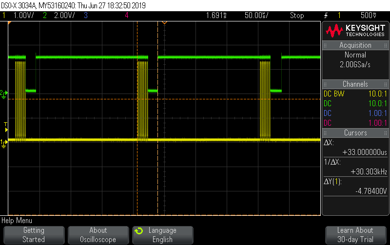
There are two ways to verify the functioning of our code. First, probing the Lock detect pin and watching the waveform over oscilloscope. Second, observing the spectrum output of the PLL. In case of the second method, insert a break-point at ‘j++’ and observe the spectrum.
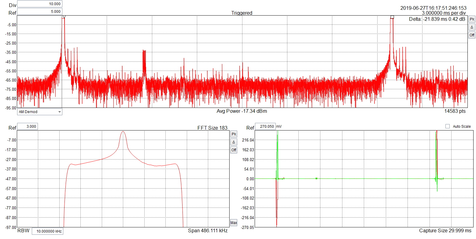
Your PLL should jump frequency in desired step size every time your code halts at the break-point. In my case, at the first halt it locks to 400MHz. Correspondingly, on the second halt it locks to 410MHz, a step delta of 10MHz as desired. This should go on for the next ‘n’ number of points.


Hi
I am new in frequency syntheses programming. I want to generate band 860 MHz to 970 MHz , 1800Mhz to 1900MhZ and 2100 MHz to 2150 Mhz.
I am using MAX2870 Board and want tp program it . please guide me at least send me the code for one band i am using arduino