
Using the Signal Integrity tool in Altium Designer – Part 1
Our designs are becoming faster to serve our ever-growing demands from machines. Speed brings more complexity to the design. The usual slow transitions from 0 to 1 and 1 to 0 become so fast that such “digital” signals have to be treated very differently. Since you are already reading this, you have some idea about what signal integrity means. In short, signal integrity is a process that tries to maintain the signal shape all the way from the transmitter to the receiver. In complex circuits having DDR memories, we get to deal with tens or even hundreds of parallel signals. Some of them need to have equal lengths, while some signals require could jump out of their lane and disturb the neighbours. Correspondingly, almost all of the signals requiring a “signal integrity” check need an impedance-controlled route for the signals to flow. The Signal Integrity tool in Altium Designer helps us run various checks on a fully or partially routed PCB to verify signal integrity on a set of signals.
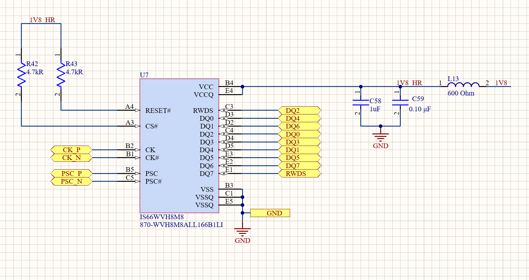
In this article, I will be trying out the Altium Designer signal integrity tool on a PCB having Lattice Crosslink-NX part and a HyperRAM.
Setting up the tool
Things get easier when you use the parameter set to define rules for a set of connections. This allows you to define a fixed set of rules on multiple connections at once and that way you don’t have to do it manually for every net.
Assigning model
First, we will set the model for the chip. You can either use a vendor-supplied IBIS model or define the IO technology yourself by doing the following.
Double-click the part > Add model > Select the desired IO technology
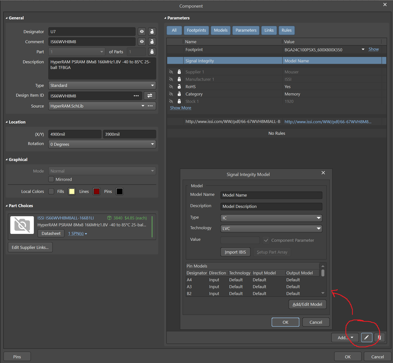
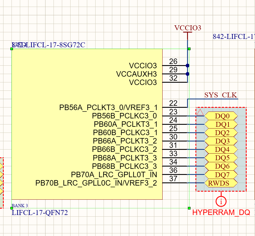
The technology could be anything that your chip supports. It could be TTL, LVCMOS, ALVC, etc. Make sure you read the part datasheet while setting this parameter. The simulation requires this data to be fed correctly for accurate results. Do the same process and assign the model to the other chip where it’s connected. In my case, this HyperRAM is connected directly to the Lattice Crosslink-NX FPGA.
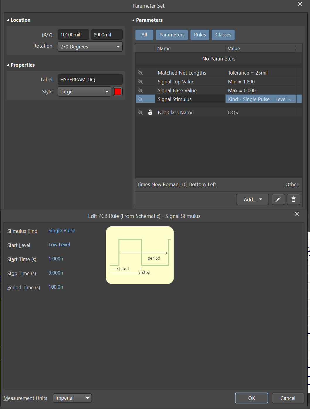
Parameter set
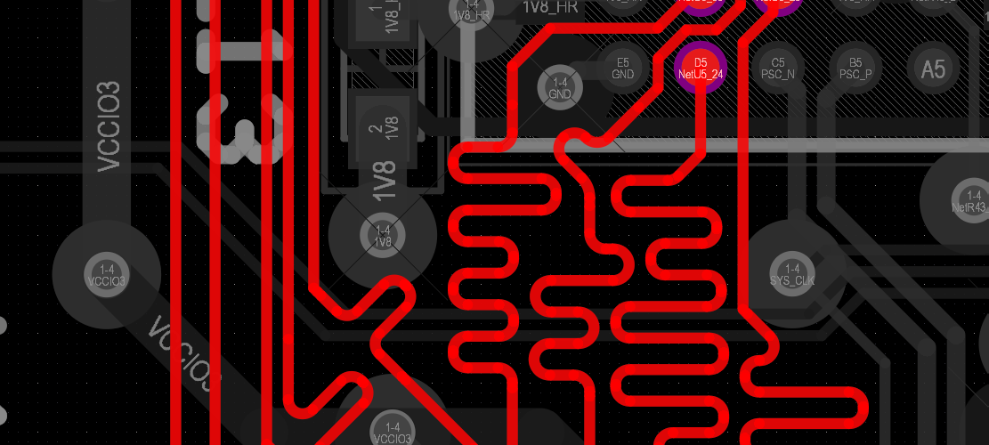
I will be using the parameter set for two reasons, one is to add the DQ nets of the memory interface to a “Net class” and the other is to assign signal integrity rules to those nets.
The marked nets must be length-matched and have good rise and fall times. For our simulation, I am using an 8ns pulse with 1ns rise and fall times.
Running the simulation
Go to Tools > Signal Integrity which will automatically ask for a model assignment. If you are confident that the part models you set are right, you can click on Continue and go to the next step. Now, for double verification, I will click on “Model assignment” and check the parameters just to be sure. You should do this at least the first time.
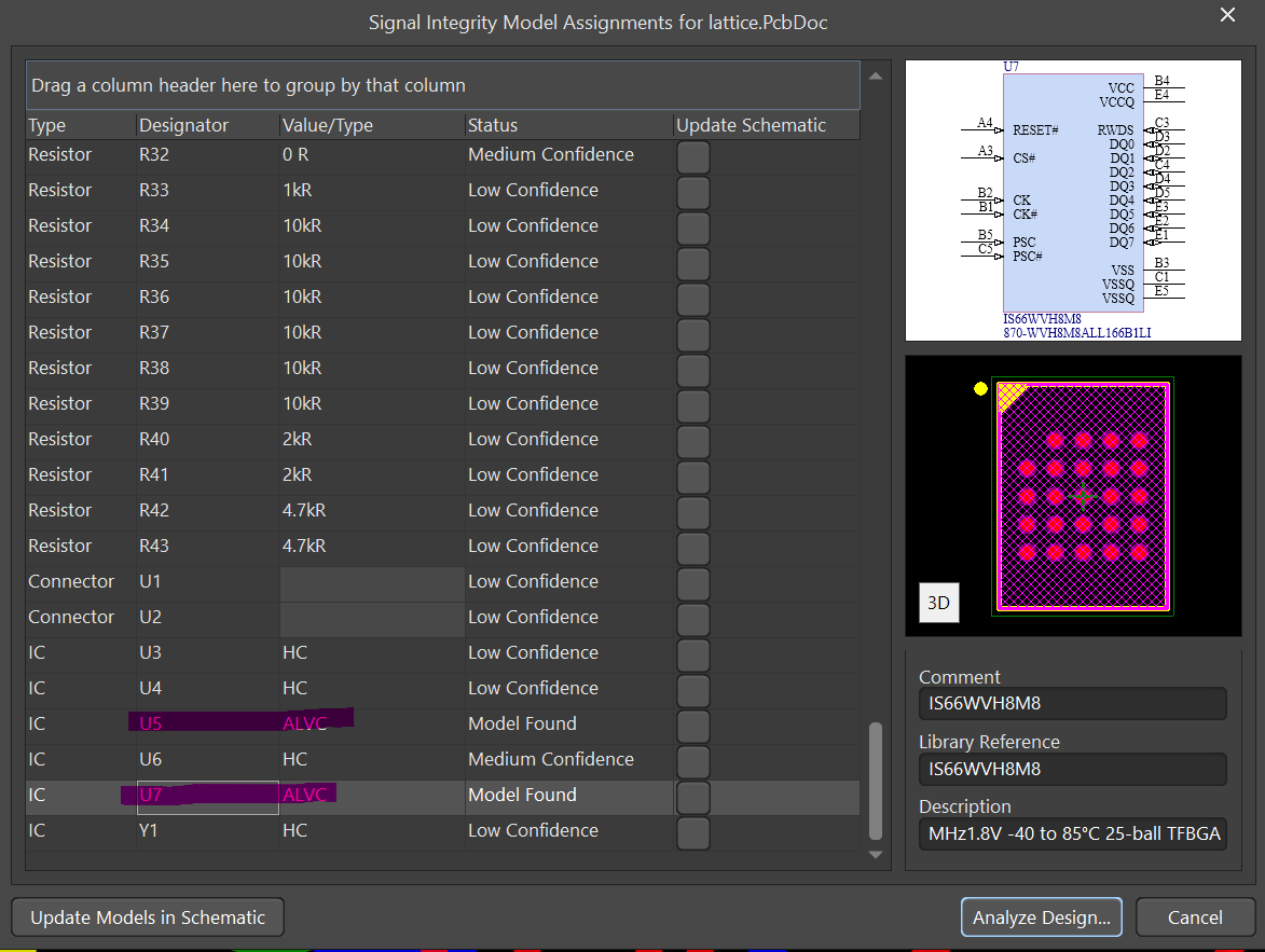
We edited our part models in schematic to ALVC technology. That reflects here correctly. Therefore, we are ready to proceed to the next step. Click “Analyze Design…”.
If you have done your PCB layout, you should see a bunch of information in the next window which we need to carefully analyze.
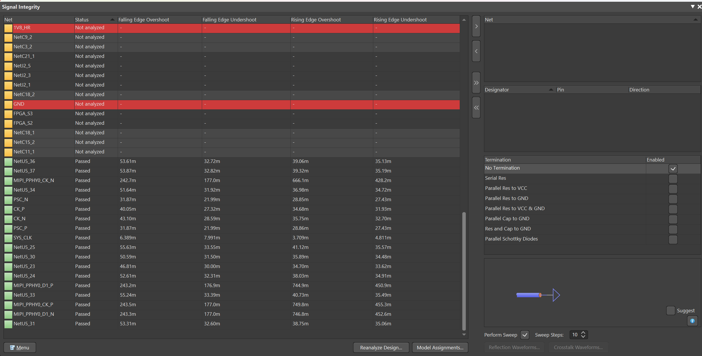
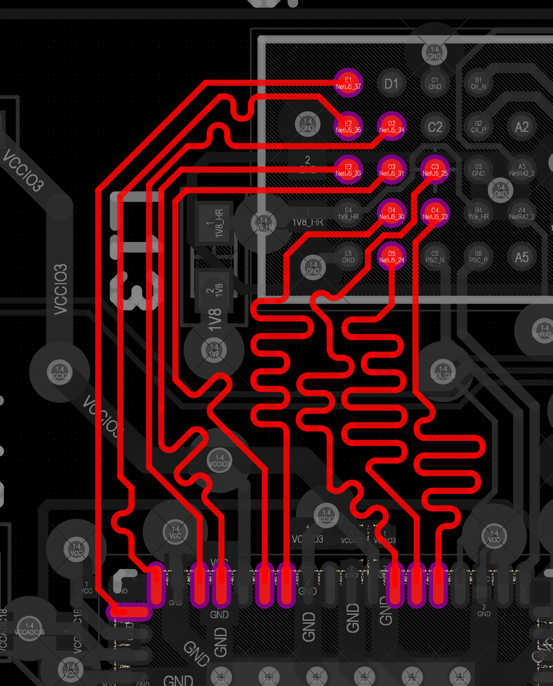
The analysis shows all the nets in the design. We are interested only in the DQS net class. The DQS net class contains all critical data lines over which data and control signal flow. I have highlighted the nets to give you an idea.
Crosstalk simulation
Let us run the “Crosstalk simulation” to understand the signal interactions along the routes. To perform the crosstalk simulation, select two or more neighbouring nets from the analysis window and click on the right arrow at the top. Choose one of the nets as the aggressor and the other net(s) as victim(s). Finally, click on “Crosstalk waveforms” to view the simulation data.
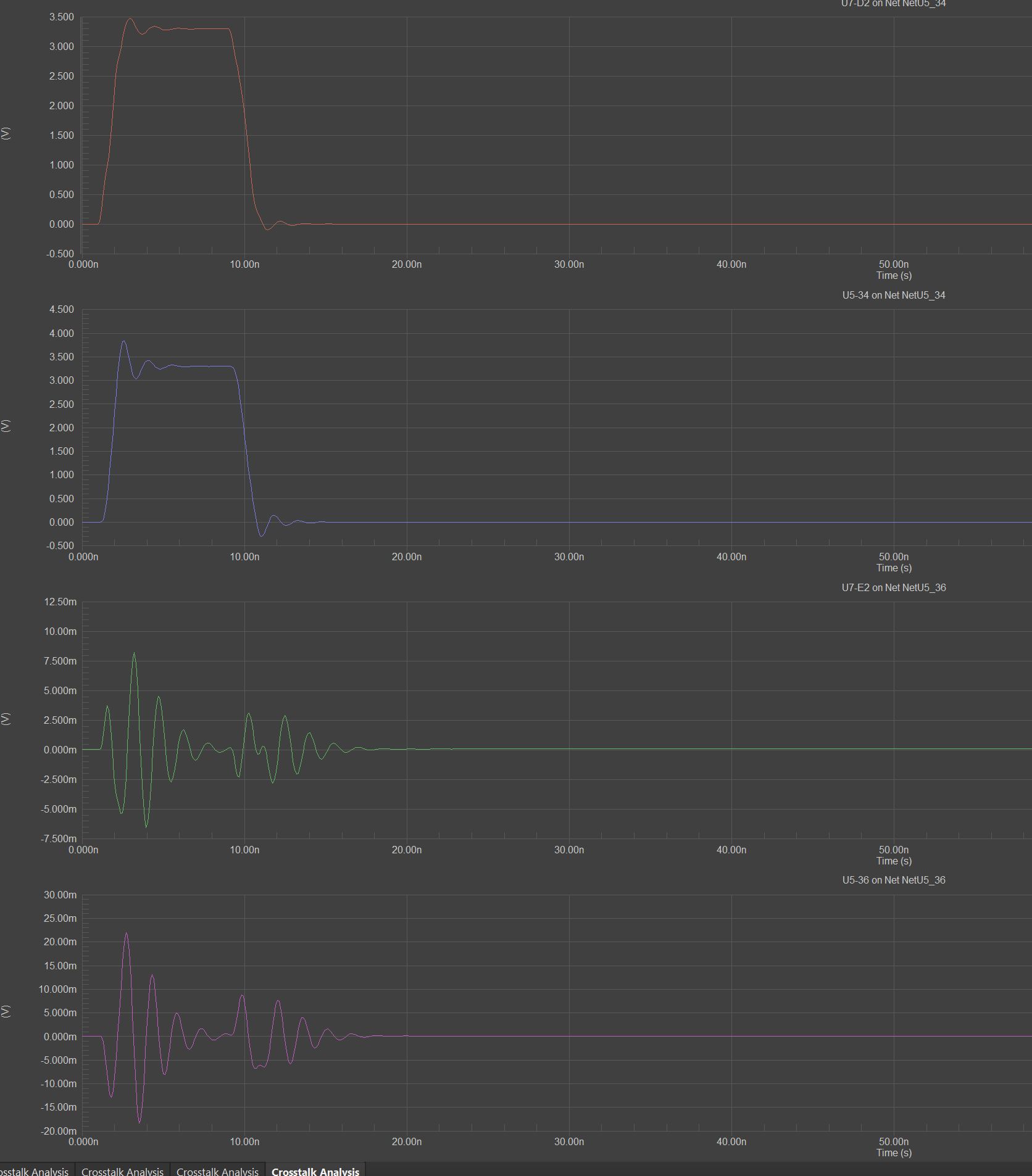
The crosstalk waveforms show the signal integrity for the given stimulus. Understanding the signal integrity and working on improving it can be a long-running process. In the above two waveforms, we observe the stimulus received on the receiving end of the route. On the other hand, the bottom two waveforms show the disturbance caused on the “Victim net” while the aggressor has stimulus applied on it.
For next time…
In the next article I will show you how to correctly analyze the waveforms and improve crosstalk performance as well as various other things to obtain best possible signal integrity in your circuit. The Signal integrity tool in Altium Designer is very useful while designing high-speed circuits. So far, we have only scratched the surface and there’s a lot more to learn in coming weeks.
Voice of the people